Various Chip Design Articles
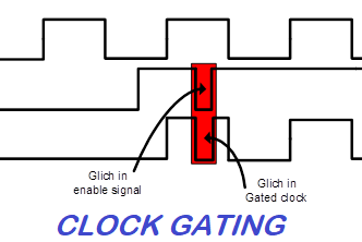
Clock Gating is defined as: “Clock gating is a technique/methodology to turn off the clock to certain parts of the digital design when not needed”.
Before continuing, be sure you're familiar with the basic concepts of MOS transistors that will prepare you for the following information. The drain/source and substrate junctions in a MOS transistor are reverse biased during transistor operation.
Several foundries continue to develop new processes based on next-generation gate-all-around transistors, including more advanced high-mobility versions, but bringing these technologies into production is going to be difficult and expensive.
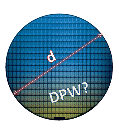
Calculating the number of Dies Per Wafer (DPW) is a very simple and straight forward task. It’s actually based on basic high school mathematics which are related to circle area formula, remember Pi?
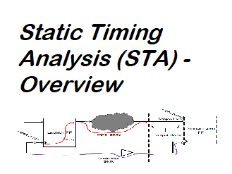
Static Timing Analysis is defined as: a timing verification that ensures whether the various circuit timing are meeting the various timing requirements. One of the most important and challenging aspect in the ASIC/FPGA design flow is timing closure.

In previous articles in this series, we looked at two important thermal performance metrics of an IC package, junction-to-thermal (or θJA) and junction-to-case (θJC) thermal resistances. We also discussed the test conditions for measuring θJA and how to design for θJC with a heat sink.
Use this online calculator to figure out die yield using Murphy's model. You'll need to know the die size, wafer diameter, and defect density. iSine is your complete resource for ASIC design - from concept to manufacturing and testing.

In the previous articles, we've discussed factors that affect the thermal performance of an IC package, including junction-to-ambient thermal resistance (θJA) (including optimal test conditions for θJA) and junction-to-case thermal resistance (θJC).

The lifetime of a semiconductor device can reduce significantly when it is operated at temperatures above the rated values. Hence, the thermal performance should be carefully evaluated both at the device and system levels.

Advanced IC packaging is a prominent technology highlight of the “More than Moore” arena. At a time when chip scaling is becoming more difficult and expensive at each node, engineers are putting multiple chips in advanced packages as an alternative to chip scaling.

Thermal performance of an IC (integrated circuit) package can be specified by several different parameters such as θJA, θJB, θJC, ΨJT, and ΨJB. A deeper understanding of these parameters can help us have a more accurate estimation of the thermal performance of our product.

In this continuation of our series on transistor sizing in VLSI, we'll go over the third and final model in our series, the linear delay model. Be sure to check out the previous articles if you'd like to learn about the linear-RC delay model and the popular Elmore delay model.

When they were first commercialized at the 22 nm node, finFETs represented a revolutionary change to the way we build transistors, the tiny switches in the “brains” of a chip.

In the last article, we discussed transistor sizing in VLSI design using the linear-RC delay model. We concluded that article by noting academics who argue this model is not the most accurate. A more accurate model is the Elmore delay model, which we will discuss here.