Thermodynamic computing isn't just a rebrand of probabilistic computing
Thermodynamic computing isn't just a rebrand of probabilistic computing

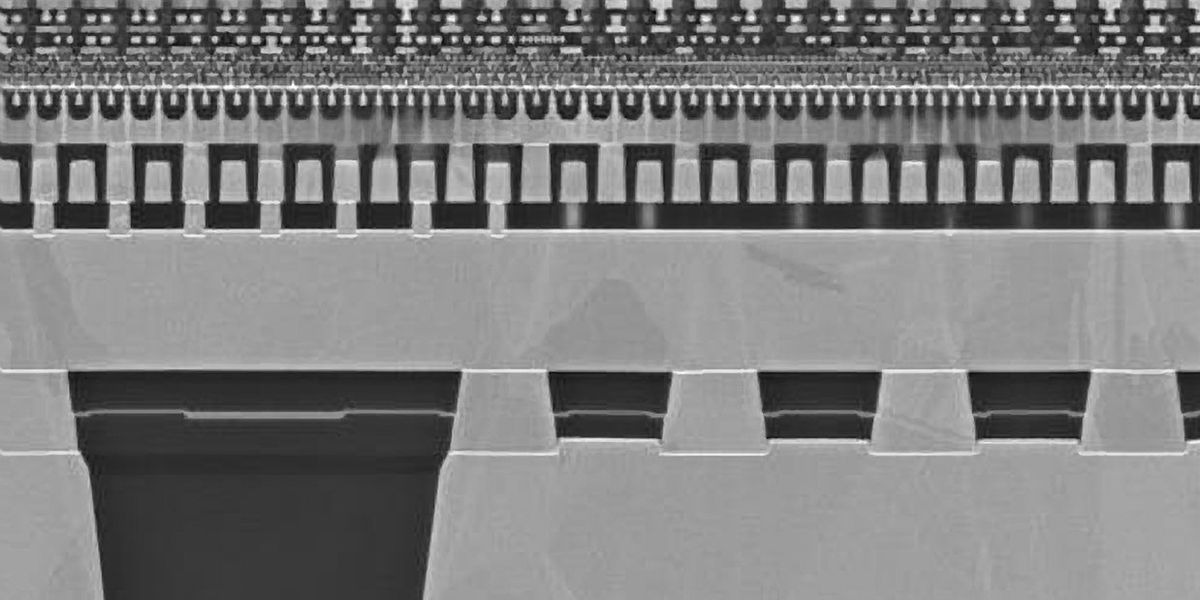
An adaptive metal fill extraction technique dynamically adjusts the level of detail based on the design context, such as the density of...

CXL 3.1 and PCIe 6.2 are transforming AI with improved data transfer and memory pooling.

Many features of UCIe 2.0 seen as “heavy” are optional, causing confusion.

Silicon is the industry standard for semiconductors. However, GaN has become a more beneficial option for RF applications.

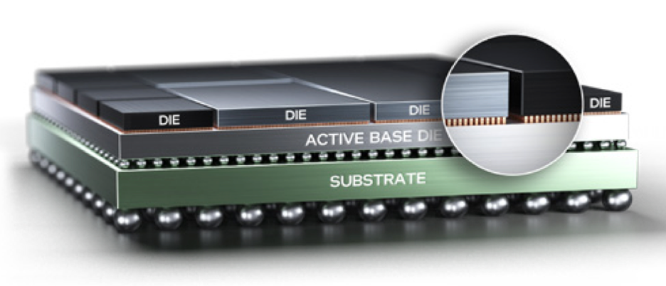
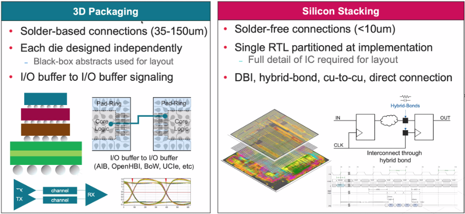
TSMC also revealed developments in advanced packaging technologies at the NA Technology Symposium, and they look interesting.

Unpacking the bear thesis on power semis and TSMC’s footnote in the story

The BSIM (Berkeley Short-channel IGFET Model) Group, located in the Department of Electrical Engineering and Computer Sciences (EECS) at the University of California, Berkeley, develops physics-based, accurate, scalable, robust, and predictive MOSFET SPICE models for circuit simulation and CMOS technology development. All suggestions for model improvements are charted by the Compact Model Coalition (CMC).

The Future of AI Accelerators: A Roadmap of Industry Leaders The AI hardware race is heating up, with major players like NVIDIA, AMD, Intel, Google, Amazon, and more unveiling their upcoming AI accelerators. Here’s a quick breakdown of the latest trends: Key Takeaways: NVIDIA Dominance: NVIDIA continues to lead with a robust roadmap, extending from H100 to future Rubin and Rubin Ultra chips with HBM4 memory by 2026-2027. AMD’s Competitive Push: AMD’s MI300 series is already competing, with MI350 and future MI400 models on the horizon. Intel’s AI Ambitions: Gaudi accelerators are growing, with Falcon Shores on track for a major memory upgrade. Google & Amazon’s Custom Chips: Google’s TPU lineup expands rapidly, while Amazon’s Trainium & Inferentia gain traction. Microsoft & Meta’s AI Expansion: Both companies are pushing their AI chip strategies with Maia and MTIA projects, respectively. Broadcom & ByteDance Join the Race: New challengers are emerging, signaling increased competition in AI hardware. What This Means: With the growing demand for AI and LLMs, companies are racing to deliver high-performance AI accelerators with advanced HBM (High Bandwidth Memory) configurations. The next few years will be crucial in shaping the AI infrastructure landscape. $NVDA $AMD $INTC $GOOGL $AMZN $META $AVGO $ASML $BESI

Huawei patented a new technology called "ternary logic" that can develop energy-efficient AI chips. The new patent confirms the company's effo

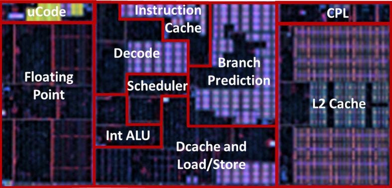
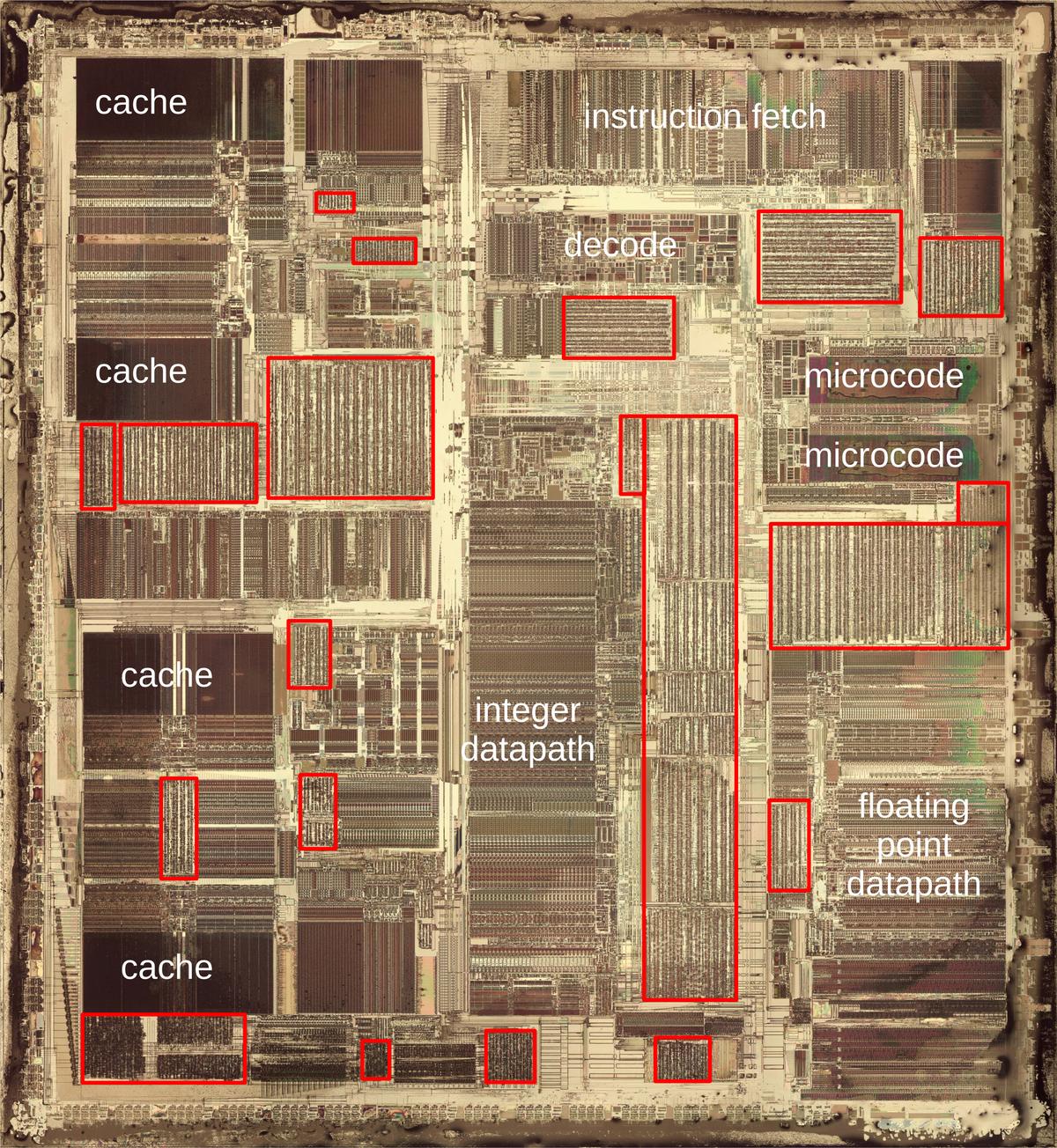
Most people think of machine instructions as the fundamental steps that a computer performs. However, many processors have another layer of ...

China’s biggest semiconductor manufacturer, SMIC, is rumored to complete 5nm chip development in 2025, leading to advanced chip orders from Huawei
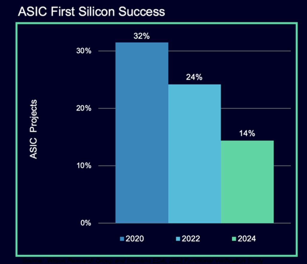
Number of designs that are late increases. Rapidly rising complexity is the leading cause, but tools, training, and workflows need to improve.
Nvidia's endorsement of co-packaged optics means the time is right

BintangChip is one of the world’s leading specialty foundry groups for analog/mixed-signal semiconductor technologies. As a pure-play foundry, we provide manufacturing and strong design support services to our customers that design analog/mixed-signal integrated circuits and other semiconductor devices for use in their own products or the products of their customers.

Pixel-level dose correction improves the quality of masks written by multi-beam.
It is often said that companies – particularly large companies with enormous IT budgets – do not buy products, they buy roadmaps. No one wants to go to

[vc_row][vc_column column_width_percent=”90″ gutter_size=”3″ overlay_alpha=”50″ shift_x=”0″ shift_y=”0″ shift_y_down=”0″ z_index=”0″ medium_width=”0″ mobile_width=”0″ width=”1/1″ uncode_shortcode_id=”158708″][vc_column_text uncode_shortcode_id=”154284″] Conventional wisdom in semiconductor manufacturing has long […]
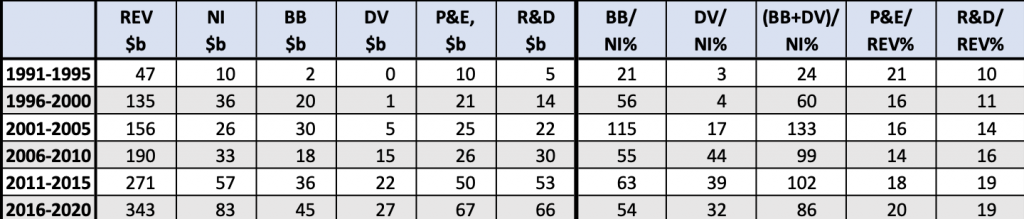
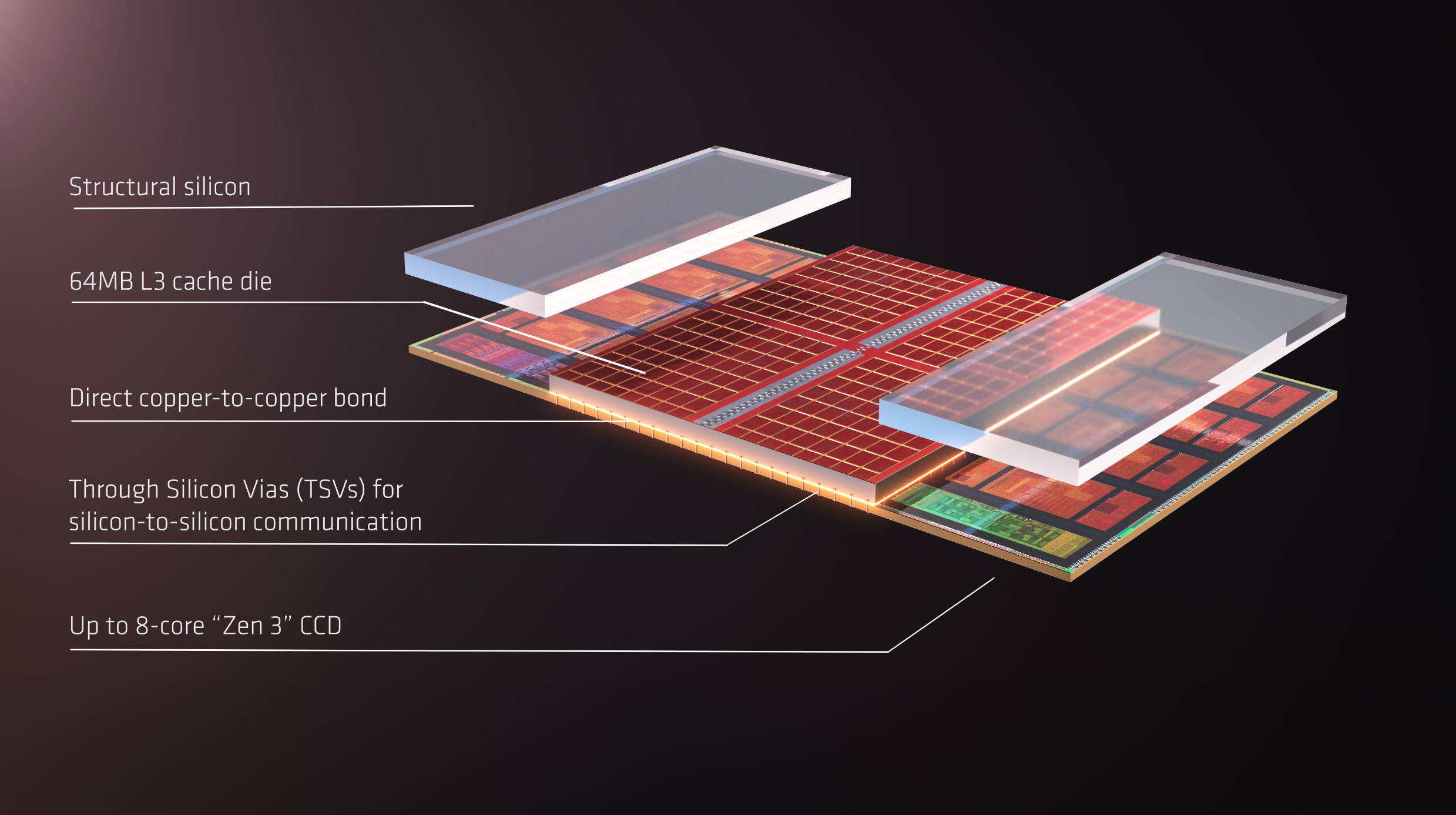
After persistent rumors refused to recede, AMD steps in with a clear explanation why dual-CCD V-Cache doesn't exist.
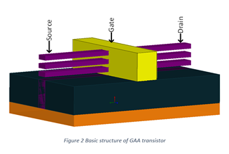
Introduction to Gate-All-Around (GAA) Transistors Gate-all-around (GAA) transistors are a newly introduced type of transistor structure: the gate terminal connects with the channel on all sides. Gate-All-Around transistors are a multi-gate field effect transistors type where a silicon nanowire gate moves around the channel by further scaling down FinFET. The Gate-All-Around structure enables a vertical

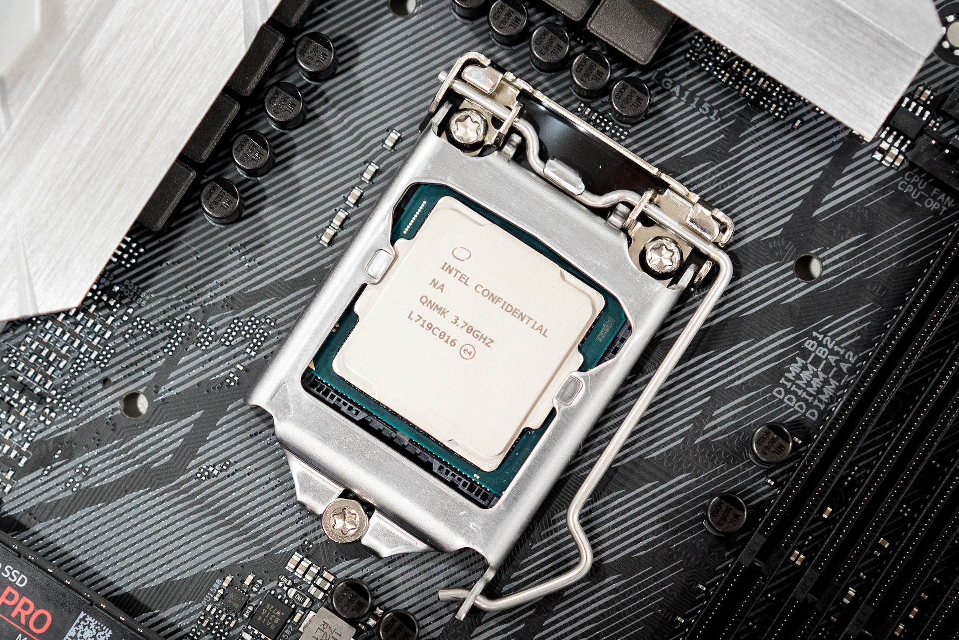
In 1993, Intel released the high-performance Pentium processor, the start of the long-running Pentium line. The Pentium had many improvement...

The CCD stack with 3D V-Cache on the AMD Ryzen 7 9800X3D is only 40-45µm in total, but the rest of the layers add up to a whopping 750µm.

Large Language Models (LLMs) have become a cornerstone of artificial intelligence, driving advancements in natural language processing and decision-making tasks. However, their extensive power demands, resulting from high computational overhead and frequent external memory access, significantly hinder their scalability and deployment, especially in energy-constrained environments such as edge devices. This escalates the cost of operation while also limiting accessibility to these LLMs, which therefore calls for energy-efficient approaches designed to handle billion-parameter models. Current approaches to reduce the computational and memory needs of LLMs are based either on general-purpose processors or on GPUs, with a combination of weight quantization and

It hasn’t achieved commercial success, but there is still plenty of development happening; analog IMC is getting a second chance.

There is no shortage of top-name – and even lesser known – companies pursuing the white whale of developing a quantum computer that can run workloads and

China has announced the development of its latest quantum system, combining the Xiaohong-504, a 504-qubit superconducting quantum chip, with the Tianyan-504 quantum computer. The breakthrough comes from China Telecom Quantum Group (CTQG), which will use the new supercomputer to boost national teleco...

A new technical paper titled “Hardware Security Failure Scenarios: Potential Hardware Weaknesses” was published by NIST. Abstract “Hardware is often assumed to be robust from a security perspective. However, chips are both created with software and contain complex encodings (e.g., circuit designs and firmware). This leads to bugs, some of which compromise security. This publication... » read more

The manipulation of mechanical strain in materials, also known as strain engineering, has allowed engineers to advance electronics over the past decades, for instance enhancing the mobility of charge ...
I was studying the silicon die of the Pentium processor and noticed some puzzling structures where signal lines were connected to the silico...

A loop buffer sits at a CPU's frontend, where it holds a small number of previously fetched instructions.

Joining the ASML Lego Collection - the TWINSCAN EXE:5000. The latest addition to you ASML Lego collection has arrived. Rick Lenssen from D&E (designer of the Lego ASML Skyline and the Lego TWINSCAN NXE:3400C) has delivered another masterpiece in technology, once again made entirely of Lego: the TWINSCAN EXE:5000.

Intel's first Arc B580 GPUs based on the Xe2 "Battlemage" architecture have been leaked & they look quite compelling.
Intel was a dominant leader in the CPU market for the better part of a decade, but AMD has seen massive success in recent years thanks to its Ryzen chips.

A combination of classical search and machine learning may be the way forward

While Intel's primary product focus is on the processors, or brains, that make computers work, system memory (that's DRAM) is a critical component for performance. This is especially true in servers, where the multiplication of processing cores has outpaced the rise in memory bandwidth (in other wor...

Nitro, Graviton, EFA, Inferentia, Trainium, Nvidia Cloud, Microsoft Azure, Google Cloud, Oracle Cloud, Handicapping Infrastructure, AI As A Service, Enterprise Automation, Meta, Coreweave, TCO

As awareness of environmental, social, and governance (ESG) issues grows, companies are adopting strategies for sustainable operations.

A new technical paper titled “Image Sensors and Photodetectors Based on Low-Carbon Footprint Solution-Processed Semiconductors” was published by researchers at Cardiff University. Abstract “This mini-review explores the evolution of image sensors, essential electronic components increasingly integrated into daily life. Traditional manufacturing methods for image sensors and photodetectors, employing high carbon footprint techniques like thermal evaporation... » read more
According to rumors, Nvidia is not expected to deliver optical interconnects for its GPU memory-lashing NVLink protocol until the “Rubin Ultra” GPU

Longtime Slashdot reader Baron_Yam writes: Memristors are the long-sought 4th fundamental circuit element. They promise analog computing capability in hardware, the ability to hold state without power, and to work with less power. A small cluster of them can replace a transistor using less space. W...
According to rumors, Nvidia is not expected to deliver optical interconnects for its GPU memory-lashing NVLink protocol until the “Rubin Ultra” GPU

Google Poxel 11s Tensor G6 codename leaks along with the Tensor G5 chip, expected to be built on TSMC's 2nm manufacturing process.

TSMC is moving to production with the NVIDIA cuLitho computational lithography platform to accelerate manufacturing of advanced semiconductor chips.

Fab Cost, WFE Implications, Backside Power Details

Breakthrough technology could help usher in 6G speed internet. Here's how it works and what it could mean for businesses.

WBG semiconductors promise to transform the automotive industry, elevating vehicle performance and sustainability to unprecedented levels.
Intel's Core Ultra 200 "Arrow Lake" Desktop CPU specifications have now been finalized and we are just a month away from the official launch.

The achievement could open a new swath of spectrum for wireless networks

This article examines the operation of the Class C power amplifier and how it compares to its Class A and Class B counterparts.

China has big plans for semiconductor industry and they include self reliance.
Transducer, Unilateral, Available and Power Gain; what they mean and how to calculate them.

Basic concepts required to understand classes of operation in power amplifiers.
Foundry competition heats up in three dimensions and with novel technologies as planar scaling benefits diminish.
When I recently interviewed Mike Clark, he told me, “…you’ll see the actual foundational lift play out in the future on Zen 6, even though it was really Zen 5 that set the table for that.” And at that same Zen 5 architecture event, AMD’s Chief Technology Officer Mark Papermaster said, “Zen 5 is a ground-up redesign of the Zen architecture,” which has brought numerous and impactful changes to the design of the core.

Poor quality thermal paste might be the reason your GPU is running hotter than usual after a certain period of time.

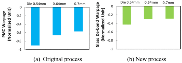
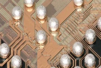
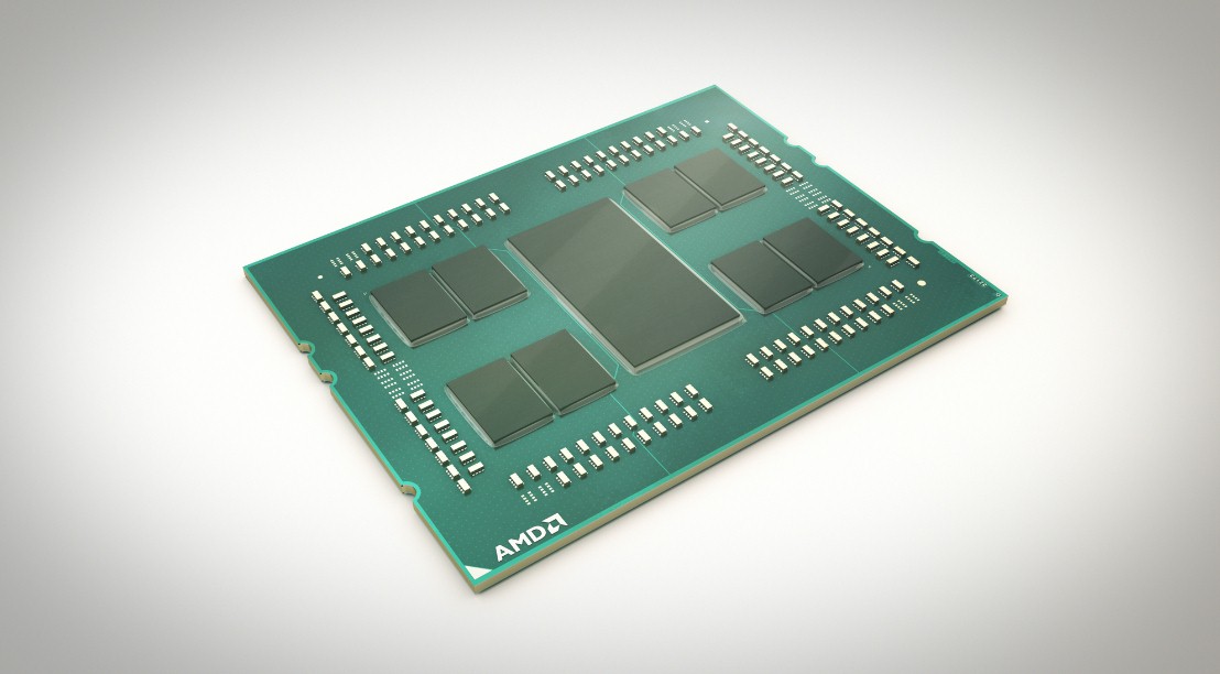
AMD reportedly plans to incorporate glass substrates into its high-performance system-in-packages (SiPs) sometimes between 2025 and 2026. Glass substrates offer several advantages over traditional organic substrates, including superior flatness, thermal properties, and mechanical strength. These cha...
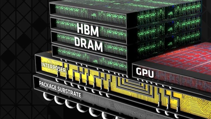
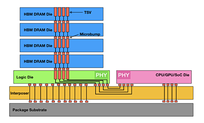
HBM4 is going to double the bandwidth of HBM3, but not through the usual increase in clock rate.

To address the limitations of GPUs for AI, engineers are exploring general-purpose hardware, dedicated DL hardware and neuromorphic hardware.
Intel released the powerful Pentium processor in 1993, a chip to "separate the really power-hungry folks from ordinary mortals." The origin...

The brain-inspired architecture gives neuromorphic systems distinct advantages, particularly for edge computing applications in consumer devices and industrial IoT.
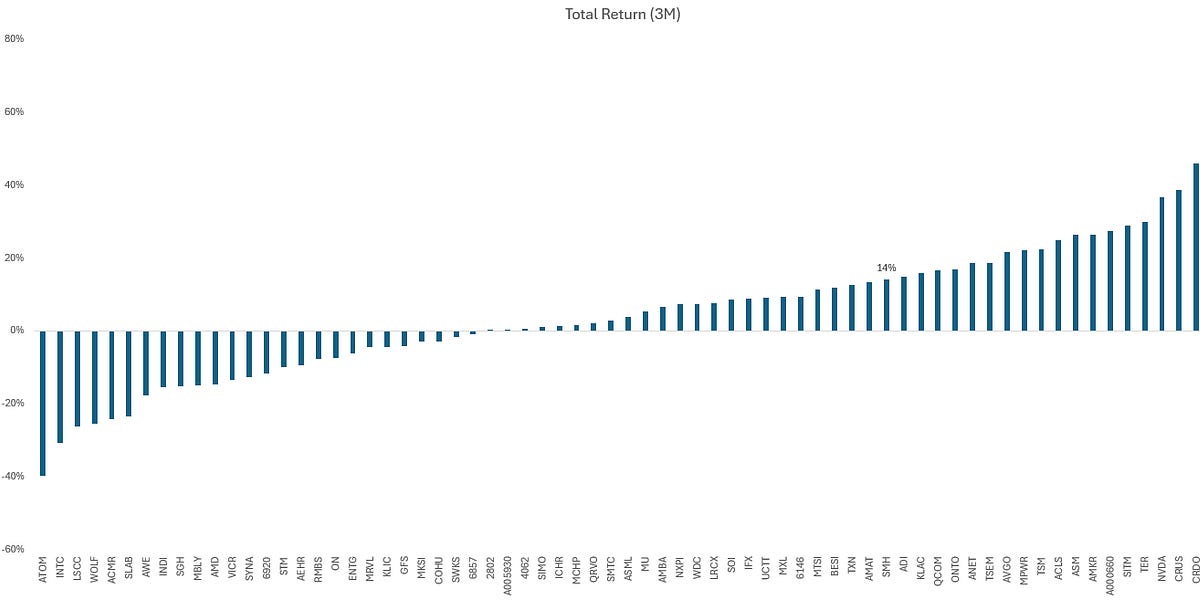
Here's everything that happened this quarter, and some thoughts and ideas.

The Sohu AI chip by Etched is a thundering breakthrough, boasting the title of the fastest AI chip to date. Its design is a testament to cutting-edge innovation, aiming to redefine the possibilities within AI computations and applications. At the center of Sohu's exceptional performance is its advanced processing capabilities, which enable it to handle complex computations at unprecedented speeds. With a capability of processing over 500,000 tokens per second on the Llama 70B model, the Sohu chip enables the creation of unattainable products with traditional GPUs. An 8xSohu server can effectively replace 160 H100 GPUs, showcasing their remarkable efficiency

Qorvo's 4 mΩ SiC JFET for solid-state circuit breakers provides significant advantages over traditional mechanical breakers. Andy Wilson discussed the details with EEPower at PCIM 2024.

Company’s new process signals transition toward foundry service provider
Mechanical stresses increase with larger sizes and heterogeneous materials.

EUV patterning has come a long way in the past five years, but old challenges resurface with high-NA EUV.
Nantian Electronics Co Limited provide complete and cost effective sourcing solution to OEMs, CEMs, distributors, the needs of manufacturers and other companies.
onsemi rises from fourth to second; top five players comprise 91.9% of revenue

Largest one-off direct foreign investment in the country

Generative AI and High Bandwidth Memory (HBM) fuel DRAM market growth. OUTLINE The HBM market has the potential to grow to US$14 billion in 2024. Yole Group expects HBM revenue growth to continue with a CAGR23-29 of ~38%, reaching about US$37.7 billion in 2029. 4F2 cell designs, hybrid bonding, and monolithic 3D DRAM will enable […]

A Finnish startup called Flow Computing is making one of the wildest claims ever heard in silicon engineering: by adding its proprietary companion chip,
In this guide, we’ll elucidate the pivotal role of FO-PLP in advancing the semiconductor sector. Harnessing cost-effectiveness with enhanced functionality, FO-PLP beckons a new era of electronic sophistication. Let’s delve into the ultimate guide to Fan-Out Panel-Level Packaging and explore how it’s shaping the future. Overview of Fan-Out Panel-Level Packaging (FO-PLP) Fan-Out Panel-Level Packaging

The semiconductor industry is set to see a record fab capacity with 17 new lines in 2025 according to Knometa Research.

With subsidies and a $6 billion acquisition, Tokyo wants to make its companies indispensable in the global supply chain.

Tech makes millions of connections in a square millimeter of silicon

Avoiding unintended shorts and opens in a high aspect ratio etch process with very tight tolerance windows.
Imagine a world where every moment is captured with immaculate clarity, from the delicate hues of a sunset to the swift action of a sporting event. The heart of this imagery revolution lies in the CMOS image sensor (CIS), a masterpiece of technology little known outside expert circles. Its evolution has been pivotal in the

Google's sixth-generation tensor processing unit (TPU) stole the company's I/O developer conference stage with its higher-than-ever computing performance.
A technical paper titled “Basilisk: Achieving Competitive Performance with Open EDA Tools on an Open-Source Linux-Capable RISC-V SoC” was published by researchers at ETH Zurich and University of Bologna. Abstract: “We introduce Basilisk, an optimized application-specific integrated circuit (ASIC) implementation and design flow building on the end-to-end open-source Iguana system-on-chip (SoC). We present enhancements to... » read more

We think that waferscale computing is an interesting and even an inevitable concept for certain kinds of compute and memory. But inevitably, the work you

Wafer dicing is a critical process within the semiconductor manufacturing. It’s the step where silicon dies are separated from each other. Semiconductor wafer dicing techniques have evolved over time, from traditional blade dicing to more advanced methods such as laser and plasma dicing, each with its own benefits and applications. Dicing Techniques

Demand for high-bandwidth memory is driving competition -- and prices -- higher

Funding round was led by SkyLake Equity Partners
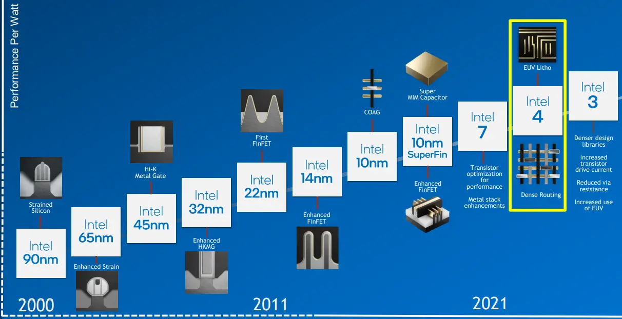
A look at Intel's next-generation high-performance process technology, Intel 4.

How High-NA EUV can be economically viable at the 1.4nm process node

Rambus has unveiled its next-gen GDDR7 memory controller IP, featuring PAM3 Signaling, and up to 48 Gbps transfer speeds.

Datacenter GPUs and some consumer cards now exceed performance limits
Beijing will be thrilled by this nerfed silicon

GPT-4 Profitability, Cost, Inference Simulator, Parallelism Explained, Performance TCO Modeling In Large & Small Model Inference and Training

Google’s new AI chip is a rival to Nvidia, and its Arm-based CPU will compete with Microsoft and Amazon
While a lot of people focus on the floating point and integer processing architectures of various kinds of compute engines, we are spending more and more

Some of the leaders of the networking industry showed up to the Optical Fiber Conference, including Broadcom, MediaTek, Semtech, and MaxLinear.
From curvilinear designs to thermal vulnerabilities, what engineers need to know about the advantages and disadvantages of photonics.
Anton Shilov reports via Tom's Hardware: About half of the processors packaged in Russia are defective. This has prompted Baikal Electronics, a Russian processor developer, to expand the number of packaging partners in the country, according to a report in Vedomosti, a Russian-language business dai...

Lenovo, the firm emerging as a driving force behind AI computing, has expressed tremendous optimism about AMD's Instinct MI300X accelerator.

The deposits formed 380 million years ago when Africa collided with North America.
Number of 8-inch SiC fabs under construction or planned globally reaches 11

The SemiAnalysis AI accelerator model is used to gauge historical and future accelerator production by company and type.
The Ethernet roadmap has had a few bumps and potholes in the four and a half decades since the 10M generation was first published in 1980. Remember the
We explore the causes and implications of asymmetric wafer defects in semiconductor manufacturing. We also consider the use of virtual process modeling to understand and mitigate these structural failures.

After coming up against the limits of physics, scientists are rethinking chip architecture like never before

We present a predictive process design kit (PDK) for the 5 nm technology node, the ASAP5 PDK. ASAP5 is not related to a particular foundry and the ass…
Startup Groq has developed an machine learning processor that it claims blows GPUs away in large language model workloads – 10x faster than an Nvidia GPU at 10 percent of the cost, and needing a tenth of the electricity. Update: Groq model compilation time and time from access to getting it up and running clarified. […]
Embracing emerging approaches is essential for crafting packages that address the evolving demands of sustainability, technology, and consumer preferences.
The discussion of any particular lithographic application often refers to…

Chafing at their dependence, Amazon, Google, Meta and Microsoft are racing to cut into Nvidia’s dominant share of the market.

In power electronics, aluminum nitride could overtake two powerhouses that only recently bested silicon

Micron’s NVDRAM chip could be a proving ground for technologies used in other products – and not become a standalone product itself. The 32Gb storage-class nonvolatile random-access memory chip design was revealed in a Micron paper at the December IEDM event, and is based on ferroelectricRAM technology with near-DRAM speed and longer-than-NAND endurance. Analysts we […]

Understanding the unique advantages provided by silicon carbide (SiC) and gallium nitride (GaN) can help you select the optimal technology to meet your products’ power, thermal, and size requirements.

China's Countermove: How Beijing is Dodging New Semiconductor Restrictions
We're getting a first glimpses of Samsung's next-generation HBM3E and GDDR7 memory chips.
This paper aims to provide insights into the thermal, analog, and RF attributes, as well as a novel modeling methodology, for the FinFET at the industry standard 5nm CMOS technology node. Thermal characterization shows that for a 165K change in temperature, the Sub-threshold Slope (SS) and threshold voltage vary by 69 % and ~70 mV, respectively. At room temperature, a single gate contacted n-FinFET RF device exhibits a cutoff and maximum oscillation frequency of ~100 GHz and ~170 GHz, respectively. Analog and RF Figures of Merit (FoMs) for 5 nm technology at a device level and their temperature sensitivity are also reported. The industry standard BSIM-CMG model is modified to capture the impact of self-heating (SH) and parasitics. The SH model is based on measured data, and the modeling approach renders it independent of other model parameters. To the authors’ knowledge, an iteration free approach to develop a model-card for RF applications is explained for the very first time. Excellent agreement between the measured data and the model indicates that our methodology is accurate and can be used for faster PDK development.

In semiconductor design, “sign-off” during the tape-out (tapeout) of a chip refers to the formal approval process to ensure that the chip design is error-free, meets all specifications, and is ready for manufacturing at the foundry. It is essential because it minimizes the risk of costly errors, ensures compliance with foundry requirements, and validates that

Join our daily and weekly newsletters for the latest updates and exclusive content on industry-leading AI coverage. Learn More Intel said it has made a significant breakthrough in the development of glass substrates for next-generation advanced packaging in an attempt to stay on the past of Moore’s Law. The big chip maker said this milestone […]
Researchers also disclosed a separate bug called “Inception” for newer AMD CPUs.
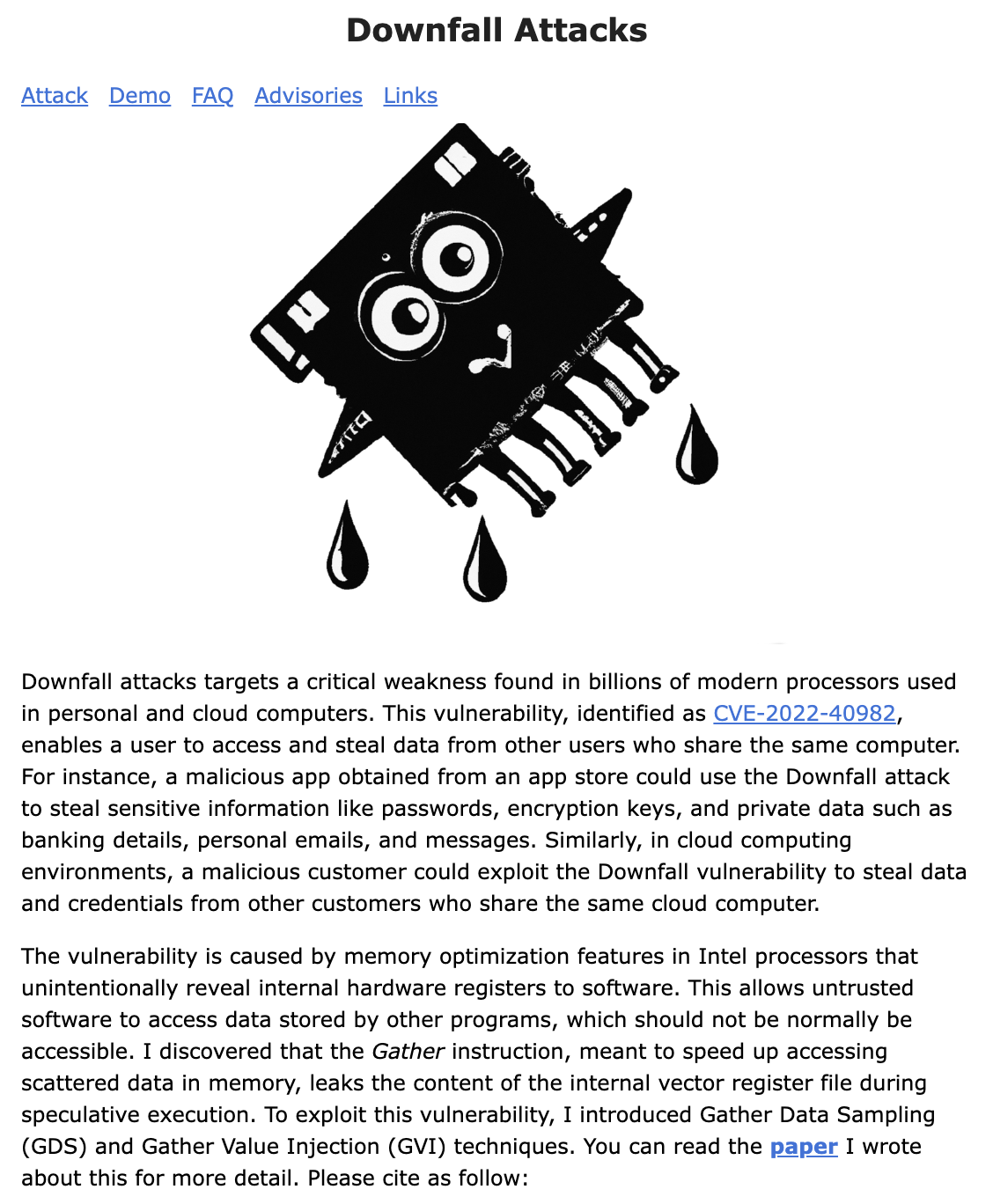
Downfall attacks targets a critical weakness found in billions of modern processors used in personal and cloud computers.

TSMC is struggling with its new 3nm process, with the semiconductor giant's yield rate reportedly far below the standard expected.
AMD, Nvidia, and Intel have all diverged their GPU architectures to separately optimize for compute and graphics.

Atom-thin layers of oxygen in a chip’s silicon can make devices speedier and more reliable

Real-time image processing is a resource-intensive task that often requires specialized hardware. With that in mind, let's explore processors that are designed specifically for photo and video applications.

The interplay between current density, temperature, and material properties.

This article introduces high-frequency conductor losses in transmission lines caused by a phenomenon known as the skin effect.

The Biden administration thinks it can preserve America’s technological primacy by cutting China off from advanced computer chips. Could the plan backfire?
Quarterly Ramp for Nvidia, Broadcom, Google, AMD, AMD Embedded (Xilinx), Amazon, Marvell, Microsoft, Alchip, Alibaba T-Head, ZTE Sanechips, Samsung, Micron, and SK Hynix

Though it'll arrive just in time for mid-cycle refresh from AMD, Nvidia, and Intel, it's unclear if there will be any takers just yet.
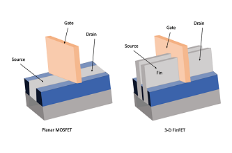
Introduction to FinFETs In the quest for smaller, faster, and more power-efficient electronic devices, the evolution of semiconductor technology has been relentless. One significant milestone in this journey has been the advent of FinFETs (Fin Field-Effect Transistors). FinFETs have emerged as a ground-breaking transistor design that has revolutionized the semiconductor industry. This article delves
The first lithography tools were fairly simple, but the technologies that produce today’s chips are among humankind’s most complex inventions.

Panmnesia has devised CXL-based vector search methods that are much faster than Microsoft’s Bing and Outlook.
PQG3-0C platform integrates optimized power and low noise transistors, PN diodes, E/D logic and RF switches on a chip to meet mmWave performance requirements
The great thing about the Cambrian explosion in compute that has been forced by the end of Dennard scaling of clock frequencies and Moore’s Law lowering

Lawsuit: Patent trolls created “harmful illusion” of unstable TV-chip market.
The company’s PowerVia interconnect tech demonstrated a 6 percent performance gain
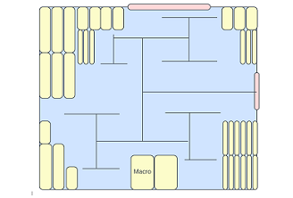
Floorplanning plays a crucial role in the physical design of an SoC and lays the foundation for an efficient and high-performance ASIC layout. In this article, we will discuss ten essential floorplanning commandments that physical design engineers can follow to ensure a correct-by-construction design. Design Partitioning Design Partitioning refers to dividing a large

GPUs may dominate, but CPUs could be perfect for smaller AI models
Tech enthusiasts probably know ARM as a company that develops reasonably performant CPU architectures with a focus on power efficiency.
Over the past 10-15 years, per-core throughput increases have slowed, and in response CPU designers have scaled up core counts and socket counts to continue increasing performance across generations of new CPU models.

Stanford team achieves first-ever optical backpropagation milestone

Google's new machines combine Nvidia H100 GPUs with Google’s high-speed interconnections for AI tasks like training very large language models.

We asked memory semiconductor industry analyst Jim Handy of Objective Analysis how he views 3D DRAM technology.
A Gainesville-based tech company is developing new ways to try to make our phones, laptops and other devices safe from bad actors.

Learn about gallium-nitride (GaN) high electron mobility transistors (HEMTs) and how they can be used in LiDAR (light detection and ranging) applications.

Vaysh Kewada, CEO and Co-Founder of Salience Labs, advances AI by circumventing finite processing power with a revolutionary new chip design.

New memory technologies have emerged to push the boundaries of conventional computer storage.
A new technical paper titled “Fundamentally Understanding and Solving RowHammer” was published by researchers at ETH Zurich. Abstract “We provide an overview of recent developments and future directions in the RowHammer vulnerability that plagues modern DRAM (Dynamic Random Memory Access) chips, which are used in almost all computing systems as main memory. RowHammer is the... » read more

Leveraging gallium nitride (GaN) technology, the latest batch of power devices boast improved performance, high efficiency, and low design costs.

Uncover design and construction weaknesses by applying increased stressors to force failures.

A new technical paper titled “RF Energy Harvesting and Wireless Power Transfer for Energy Autonomous Wireless Devices and RFIDs” was published by researchers at Institut Polytechnique de Paris, Universidade de Aveiro, The Hague, McGill University, University of Bordeaux, Polytechnique Montreal, and others. Abstract: “Radio frequency (RF) energy harvesting and wireless power transmission (WPT) technologies —both... » read more

You can make many things with silicon photonics, but a laser is not one of them
A new technical paper titled “TPU v4: An Optically Reconfigurable Supercomputer for Machine Learning with Hardware Support for Embeddings” was published by researchers at Google. Abstract: “In response to innovations in machine learning (ML) models, production workloads changed radically and rapidly. TPU v4 is the fifth Google domain specific architecture (DSA) and its third supercomputer... » read more

Samsung Electronics has stepped up its deployment in the fan-out (FO) wafer-level packaging segment with plans to set up related production lines in Japan, according to industry sources.
While microprocessors are used in various applications, they are precluded from the use in high-energy physics applications due to the harsh radiation present. To overcome this limitation a...
In the march to more capable, faster, smaller, and lower…

Study tries to settle a bitter disagreement over Google’s chip design AI
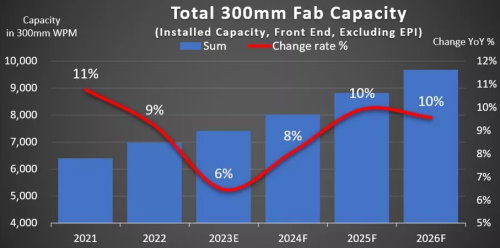
After dipping this year, the growth of 300mm semiconductor manufacturing capacity is set to gain momentum.
It was only a matter of time, perhaps, but the skyrocketing costs of designing chips is colliding with the ever-increasing need for performance,
While terms often are used interchangeably, they are very different technologies with different challenges.

RDL, an abbreviation for Redistribution Layer, that is, to make one or more layers of metal on the active chip side to redistribute the pins of the chip.
Historically Intel put all its cumulative chip knowledge to work advancing Moore's Law and applying those learnings to its future CPUs. Today, some of

Intel's multi-die interconnect bridge (EMIB) is an approach to in-package high-density interconnect of heterogeneous chips.

Powered by the promises of the CHIPS Act, Intel is investing more than $100 billion to increase domestic chip manufacturing capacity and capabilities.

USC researchers have announced a breakthrough in memristive technology that could shrink edge computing for AI to smartphone-sized devices.
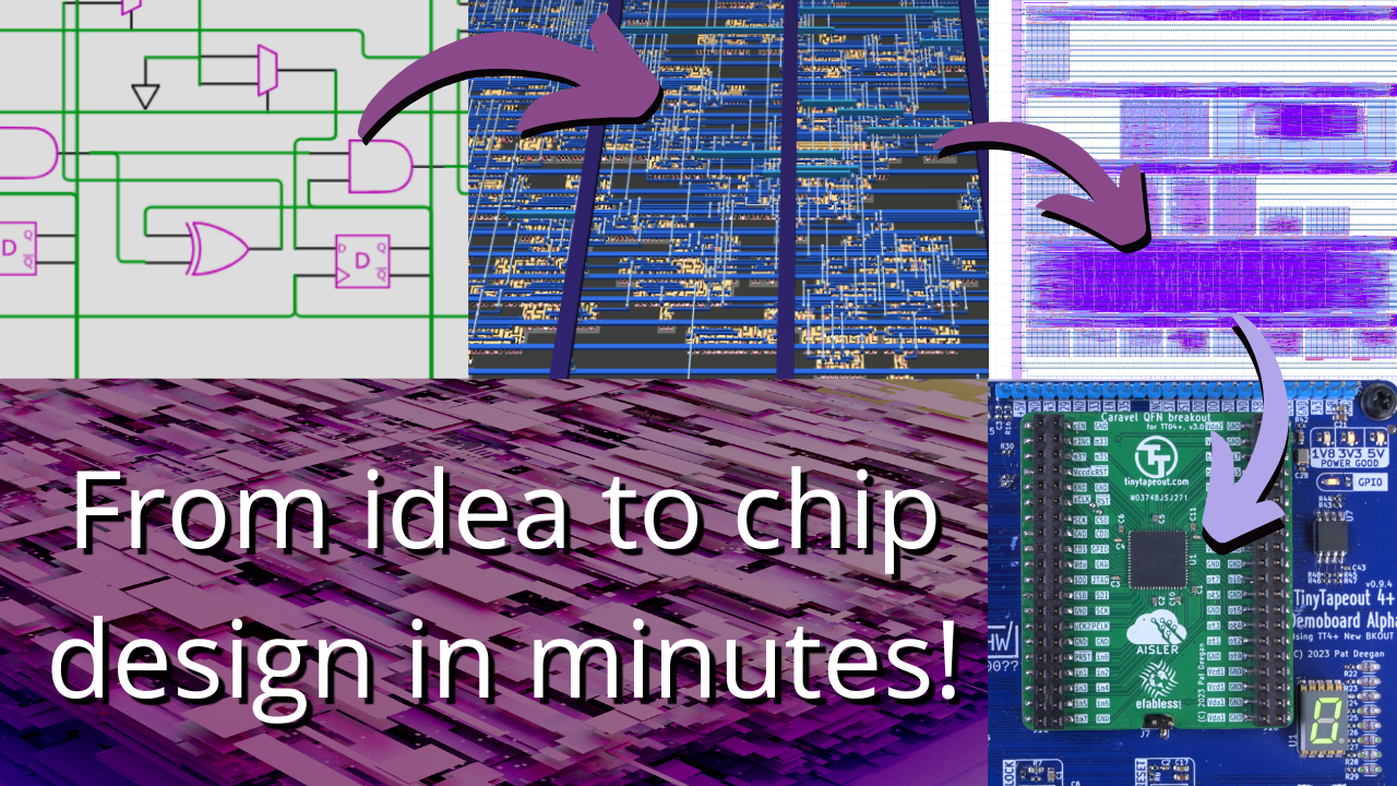
From idea to chip design in minutes! TT09 Closes in TT09 Closes in 44 DAYS 44 HOURS 44 MINS 44 SECS Tiles PCBs Tiny Tapeout is an educational project that makes it easier and cheaper than ever to get your designs manufactured on a real chip! Read the paper here. See what other people are making by taking a look at what was submitted on our previous shuttles.

Mike Wheatley / SiliconANGLE: Cerebras open sources seven GPT-based LLMs, ranging from 111M to 13B parameters and trained using its Andromeda supercomputer for AI, on GitHub and Hugging Face

Regardless of which one wins, they will cut greenhouse gases by billions of tonnes
As the US boosts production of silicon chips, an American journalist goes inside TSMC, the mysterious Taiwanese company at the center of the global industry.

A new way of making wafer-scale electronics out of atomically thin sheets.

Comprehensive up-to-date news coverage, aggregated from sources all over the world by Google News.

Chinese chip designer Loongson, which has tried to reduce the country’s reliance on Intel and AMD, is developing its own general-purpose GPU despite being added to a US trade blacklist.
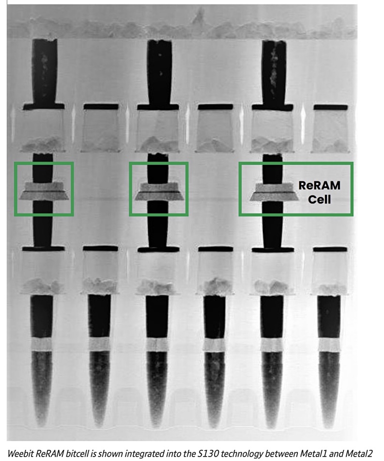
ReRAM startup Intrinsic Semiconductor Technologies has raised $9.73 million to expand its engineering team and bring its product to market.
Lead SiC test & burn-in customer boosting production of power devices for EVs
A list of artificial intelligence used in semiconductor manufacturing tools from February 2023.
China-based semiconductor manufacturers, in the wake of geopolitical risks, are expected to keep up with their capacity expansion strategies going into 2023 with a good number of projects already in construction, according to DIGITIMES Research's latest report covering the latest status of China's wafer foundry industry

Mar. 13, 2023 —- According to TrendForce’s latest survey of the global foundry market, electronics brands began adjusting their inventories in 2Q22, but foundries were unable to rapidly adapt to this development because they reside in the more upper portion of the supply chain. Moreover, revising procurement quantities of long-term foundry contracts takes time as well. Hence,

Kuo-Hua Chou, special to DIGITIMES Asia
Marvell has had a large and profitable I/O and networking silicon business for a long time, but with the acquisitions of Inphi in October 2020 and of

A new technical paper titled “APOSTLE: Asynchronously Parallel Optimization for Sizing Analog Transistors Using DNN Learning” was published by researchers at UT Austin and Analog Devices. Abstract “Analog circuit sizing is a high-cost process in terms of the manual effort invested and the computation time spent. With rapidly developing technology and high market demand, bringing... » read more

It may be the only way to keep up with environmental power regulations
The $10,000 Nvidia A100has become one of the most critical tools in the artificial intelligence industry,

AI firm Synopsys has announced that its DSO.ai tool has successfully aided in the design of 100 chips, and it expects that upward trend to continue.
We have been very public about how reliable Samsung SSDs have been in the past, so we wanted to explain why we are now moving part of our line to Sabrent.
New applications require a deep understanding of the tradeoffs for different types of DRAM.
Security IP cores are blocks that provide security features for integrated circuits (ICs) and systems-on-chips (SoCs). It includes encryption, decryption, authentication, and key management functions that protect against unauthorized access or hacking. The IP core can be integrated into a larger IC design to provide enhanced security for applications such as IoT devices, payment systems,
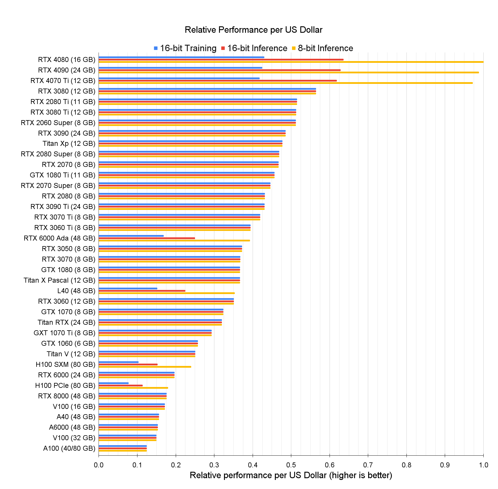
Here, I provide an in-depth analysis of GPUs for deep learning/machine learning and explain what is the best GPU for your use-case and budget.
If a few cores are good, then a lot of cores ought to be better. But when it comes to HPC this isn’t always the case, despite what the Top500 ranking –

Covering EUV Lithography, ASML, and everything in between from how it all works to their impact on the world and what it all means.
Book repository "Analysis and Design of Elementary MOS Amplifier Stages" - bmurmann/Book-on-MOS-stages
— RetiredEngineer® (@chiakokhua)

The following is a list of my articles on various topics. Besides technical articles, news pieces that might have useful technical information are also included. You can find my articles on FPGA...

Learn about voltage waves and how they relate to an important basic concept of radio frequency (RF) circuit design: transmission lines.

Industry sources say TSMC is considering lowering 3nm prices to stimulate interest from chip designers
High performance and high transistor density come at a cost

Interconnects—those sometimes nanometers-wide metal wires that link transistors into circuits on an IC—are in need of a major overhaul. And as chip fabs march toward the outer reaches of Moore’s Law, interconnects are also becoming the industry’s choke point.
Book repository "Analysis and Design of Elementary MOS Amplifier Stages" - bmurmann/Book-on-MOS-stages
List of awesome open source hardware tools, generators, and reusable designs - aolofsson/awesome-opensource-hardware

A technical paper titled “Beware of Discarding Used SRAMs: Information is Stored Permanently” was published by researchers at Auburn University. The paper won “Best Paper Award” at the IEEE International Conference on Physical Assurance and Inspection of Electronics (PAINE) Oct. 25-27 in Huntsville. Abstract: “Data recovery has long been a focus of the electronics industry... » read more
Gallium arsenide (GaAs) technology is a type of semiconductor material used in the manufacturing of various electronic devices. It is known for its high electron mobility, which allows it to operate at higher speeds and with lower power consumption compared to other semiconductor materials such as silicon.
Conventional wisdom says that trying to attach system memory to the PCI-Express bus is a bad idea if you care at all about latency. The further the memory

A new technical review paper titled “Carbon nanotube transistors: Making electronics from molecules” was published by researchers at Duke University, Northwestern University, and Stanford University. “Between the opportunities in high-performance digital logic with the potential for 3D integration and the possibilities for printed and even recyclable thin-film electronics, CNT transistors warrant a renewed and even... » read more

Why and when it's needed, and what tools and technologies are required.

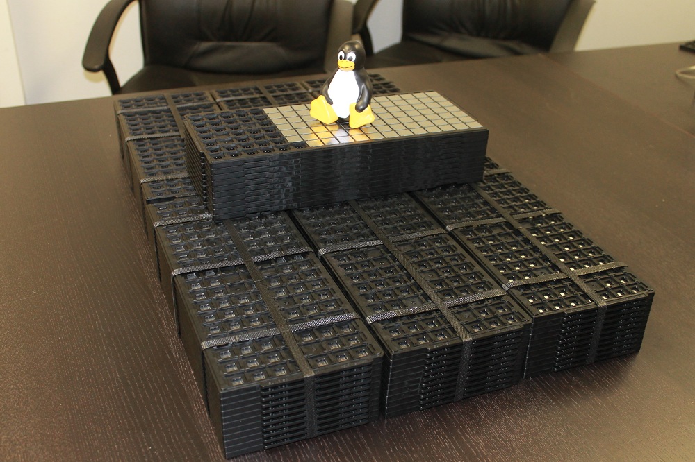
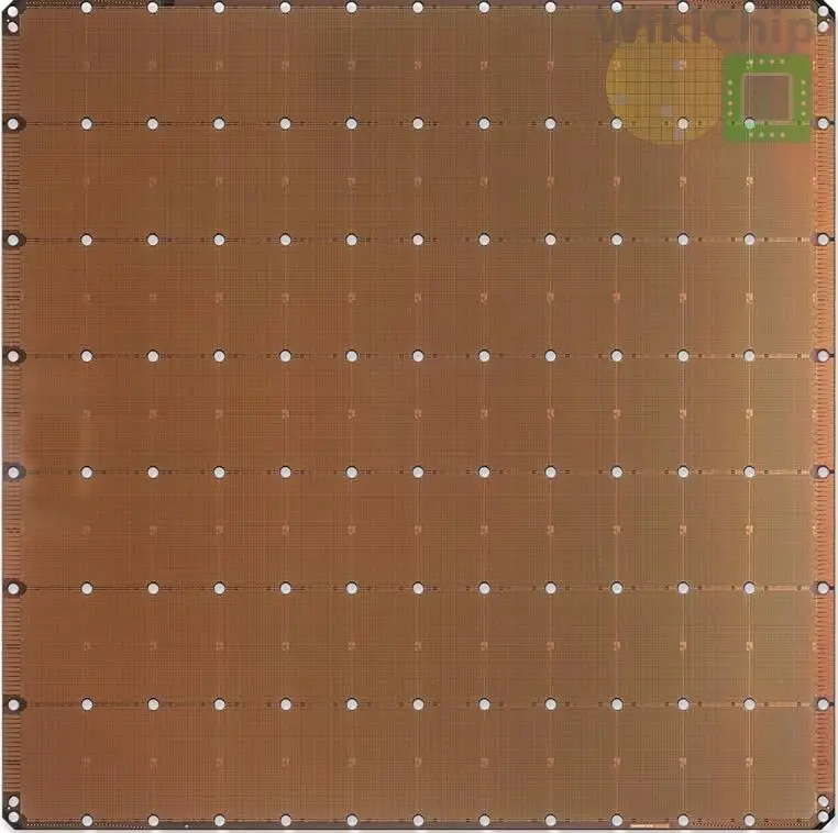
The world's largest chip scales to new heights.

Eliyan is emerging from stealth mode, unveiling the successful tapeout of its high-performance UCIe-compliant die-to-die interconnect technology in 5 nm process.

To ensure that designers have the right tools for the job, TSMC announced a slew of EDA tool certifications for its most advanced processes—ranging from 3 nm nodes to 3D semiconductor integration.
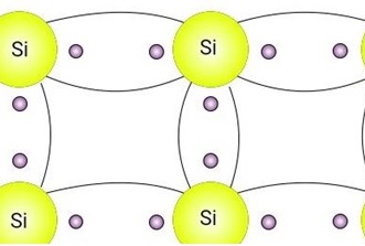
Extrinsic semiconductors have been doped with specific chemicals. This process helps to modify the electrical properties of a relatively pure semiconductor crystal.
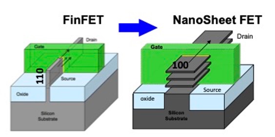
Advanced etch holds key to nanosheet FETs; evolutionary path for future nodes.

The latest American trade restrictions could significantly set back China’s semiconductor ambitions.

Using new materials, UPenn researchers recently demonstrated how analog compute-in-memory circuits can provide a programmable solution for AI computing.
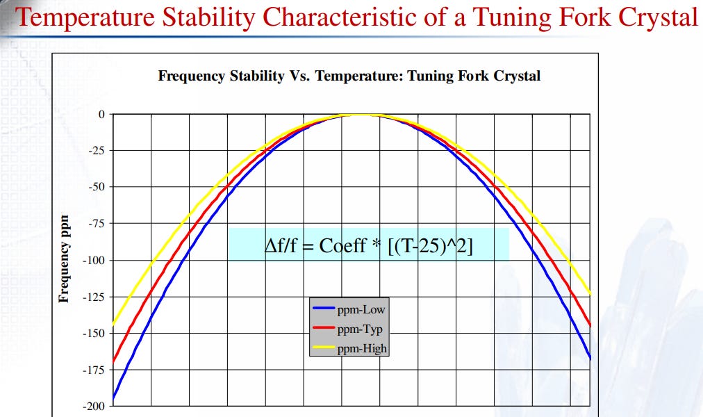
How do we keep track of time? A deeper look into Quartz timers and the emerging field of MEMS

A new technical paper titled “HiRA: Hidden Row Activation for Reducing Refresh Latency of Off-the-Shelf DRAM Chips” was published by researchers at ETH Zürich, TOBB University of Economics and Technology and Galicia Supercomputing Center (CESGA). Abstract “DRAM is the building block of modern main memory systems. DRAM cells must be periodically refreshed to prevent data... » read more
Changes are steady in the memory hierarchy, but how and where that memory is accessed is having a big impact.
A vast majority of modern digital integrated circuits are synchronous designs. They rely on storage elements called registers or flip-flops, all of which change their stored data in a lockstep manner with respect to a control signal called the clock. In many ways, the clock signal is like blood flowing through the veins of a

Long Term agreements, particularly the NCNR order is a relative newcomer this cycle. Let's see how they are holding up. The Industry Structure is showing that Fabs are in charge.

Our analysis of 14 popular consumer devices found most could stop working in 3 to 4 years because of irreplaceable batteries. Here’s how we get the tech industry to design products that last longer — and do less damage to the environment.

Google announced in a blog on August 3 that GlobalFoundries (GF) is participating in its open-source silicon initiative as a new partner, calling the new partnership a milestone in the foundry ecosystem market.

Google is promoting the growth of open source tools for designing semis. The science fiction version of this story leads to everyone designing chips, the reality is going to be much narrower, but s…

Over the last two years, Google and SkyWater Technology have partnered to make building open silicon accessible to all developers

R&D leaders can boost productivity by using advanced analytics to create stronger, faster engineering teams.

Both companies are rolling out mitigations, but they add overhead of 12 to 28 percent.

Moore's law has slowed down and, with the rise of data-intensive applications, like machine learning, new approaches to computing hardware are needed. The perspective explores the role of memristive,...

Let's learn more about the world's most important manufactured product. Meaningful insight, timely analysis, and an occasional investment idea.
Ayar Labs solves bandwidth and power bottlenecks by moving data using light. We built the world's first optical I/O chiplets.

Intel® Silicon Photonics combines the manufacturing scale and capability of silicon with the power of light onto a single chip.

Intel Lab researchers push photonics one step further by demonstrating a tightly controlled, highly integrated eight-wavelength laser.

Intel has demonstrated an eight-wavelength laser array on a silicon wafer paving the way for the next generation of integrated silicon photonics products.

Microelectromechanical systems (MEMS) vibratory gyroscopes can be a bit mysterious and math-intensive. Let's break the math down, and go over gyroscope basics and structures.

Get a high-level introduction to how standards play into the EE world.
Hertzbleed attack targets power-conservation feature found on virtually all modern CPUs.
PCI-SIG has drafted the PCIe 7.0 spec and aims to finalize it in 2025.

The high frequencies and data rates involved in 5G designs makes layout verification all the more important.
Challenge to create GaN-based 400V photovoltaic power supply
New technical paper titled “Bridging the Gap between Design and Simulation of Low-Voltage CMOS Circuits” from researchers at Federal University of Santa Catarina, Brazil. Abstract “This work proposes a truly compact MOSFET model that contains only four parameters to assist an integrated circuits (IC) designer in a design by hand. The four-parameter model (4PM) is... » read more

New technical paper titled “A Review on Transient Thermal Management of Electronic Devices” from researchers at Indian Institute of Technology Bombay. Abstract “Much effort in the area of electronics thermal management has focused on developing cooling solutions that cater to steady-state operation. However, electronic devices are increasingly being used in applications involving time-varying workloads. These... » read more

Star Trek's glowing circuit boards may not be so crazy

The researchers are considered a key to the company’s future. But they have had a hard time shaking infighting and controversy over a variety of issues.

When you’re baking a cake, it’s hard to know when the inside is in the state you want it to be. The same is true—with much higher stakes—for microelectronic chips: How can engineers confirm that what’s inside has truly met the intent of the designers? How can a semiconductor design company tell wh
Target is 20kV, to protect electric grid from electromagnetic pulse
Challenges and troubleshooting employed to design a 2048-chiplet, 14,336-core waferscale processor system.

Semiconductor Engineering's collection of technical papers for the chip industry.

In 2004 I was working for Microsoft in the Xbox group, and a new console was being created. I got a copy of the detailed descriptions of the Xbox 360 CPU and I read it through multiple times and su…
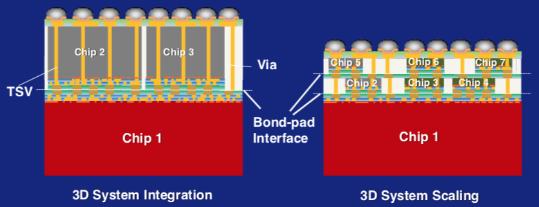
There are two types of packaging that represent the future of computing, and both will have validity in certain domains: Wafer scale integration and

The firm pivoted away from riskier spiking neural networks using a new power management scheme

EE Times Compares SRAM vs. DRAM, Common Issues With Each Type Of Memory, And Takes A Look At The Future For Computer Memory.
An integrated cache and memory access time, cycle time, area, leakage, and dynamic power model - HewlettPackard/cacti

This article looks at gallium arsenide, comparing it to other semiconductor materials, and explores how different compounds are used in components.
As we previously reported, Google unveiled its second-generation TensorFlow Processing Unit (TPU2) at Google I/O last week. Google calls this new

What are TMR sensors and what applications are they best suited to? This article provides a snapshot of this sensor type and what TMR-based components are available for designers.
Nvidia has staked its growth in the datacenter on machine learning. Over the past few years, the company has rolled out features in its GPUs aimed neural
Four years ago, Google started to see the real potential for deploying neural networks to support a large number of new services. During that time it was
D&R provides the world's largest directory of Silicon IP (Intellectual Property), SoC Configurable Design Platforms and SOPC Products from 400 vendors

This article will help the reader understand the different types of power semiconductors: how they work, their key parameters, and trade-offs.
The modern GPU compute engine is a microcosm of the high performance computing datacenter at large. At every level of HPC – across systems in the

PARIS — If you’ve ever seen the U.S. TV series “Person of Interest,” during which an anonymous face in the Manhattan crowd, highlighted inside a digital
This blog post is in response to a recent topic on the Parallella forum regarding Adapteva’s chip cost efficiency (GFLOPS/$): [forum discussion thread]. I had to be a little vague on some poi…
Explore semiconductor IP, white papers, news, technical articles and more from hundreds of top semiconductor IP vendors and foundries.
Magic VLSI: Resource Page

An effective interconnect makes delivering a complex SoC easier, more predictable, and less costly.

Explore Synopsys Blog for the latest insights and trends in EDA, IP, and Systems Design. Stay updated with expert articles and industry news.

Innovative new clocking schemes in the latest LPDDR standard enable easier implementation of controllers and PHYs at maximum data rate as well as new options for power consumption.

5G Beamforming Antennas Create Design, Test Problems Assuring quality under changing conditions with shifting standards and use models is a major challenge.
I have written a lot of articles looking at leading…
Currently there are more than 100 companies all over the world building ASIC’s (Application specific integrated circuit) or SOC’s (System…

This article introduces a phase-based feedback system that plays an important role in many applications.

How to build a multi-chip neural model with minimal overhead.

This tutorial describes methods to enable efficient processing for deep neural networks (DNNs), which are used in many AI applications including computer vision, speech recognition, robotics, etc....

Getting data in and out of memory faster is adding some unexpected challenges.
PALO ALTO, Calif., August 19, 2019 — UPMEM announced today a Processing-in-Memory (PIM) acceleration solution that allows big data and AI applications to run 20 times faster and with 10 […]

Experts at the Table: Which type of DRAM is best for different applications, and why performance and power can vary so much.

Evaluate inference accelerators to find the best throughput for the money.

Cheaper than gallium arsenide. More flexible band-gap tuning than silicon. What's silicon germanium's place in circuit design?

Lidar is essential for self-driving cars—here’s how some leading lidar sensors work.

This technical brief attempts to dispel some of the fog surrounding the three-character naming convention used to describe ceramic caps.

This article will discuss the basic concepts of clock gating and how it can be used to reduce the power consumption of synchronous digital systems.
The new technology is 10 times as reliable as what's come before for keeping internet-connected devices secure.

We talked to lidar company executives and independent experts.

This article focuses on using Verilog to describe synchronous sequential circuits.

Emerging memory technologies call for an integrated PVD process system capable of depositing and measuring multiple materials under vacuum.

This article explains how a PLL can be used to produce a high-frequency clock from a low-frequency reference signal.

Review whitepapers written by our expert engineers to help you understand new concepts or implement best practices in your product design and development.

This article will take a closer look at the commands used to control and interact with DRAM.
An essay that bids farewell to x87 – a computing architecture too long for this world.
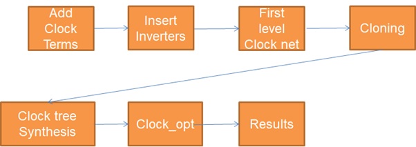
SoC clock tree overview, metrics that help qualify a clock tree and most commonly used clock tree distribution methodologies.

A probe card is essentially an interface or a board that is used to perform wafer test for a semiconductor wafer. It is used to connect to the integrated circuits located on a wafer to the ATE (Automated Test Equipment) in order to test their electrical parameters and performance before they are manufactured and shipped

Learn more on the various capacitors in ASIC design that can improve your chip performance and recude it's cost.
File formats used by EDA tools.
Software optimization manuals for C++ and assembly code. Intel and AMD x86 microprocessors. Windows, Linux, BSD, Mac OS X. 16, 32 and 64 bit systems. Detailed descriptions of microarchitectures.
Standard Test Data Format (STDF) is a proprietary file format for semiconductor test information originally developed by Teradyne, but it is now a de facto standard widely used throughout the semiconductor industry. It is a commonly used format produced by automatic test equipment (ATE) platforms from companies such as Cohu, Roos Instruments, Teradyne, Advantest, SPEA S.p.A, and others.

Over the last two years, there has been a push for novel architectures to feed the needs of machine learning and more specifically, deep neural networks.
The lack of stability is one of the major limitations that constrains PUF from being put in widespread practical use. In this paper, we propose a weak PUF and a strong PUF that are both completely...
Read the latest Analog Electronic & Electrical Engineering Technical Articles

This article introduces the techniques for describing combinational circuits in Verilog by examining how to use the conditional operator to describe combinational truth tables.

This article will take a deeper look at five key power supply problems, how to know when they arise, and the best ways to address or mitigate them.
In the battle of bandwidth and compute, Cloudflare has a strong hand. A dive into networking infrastructure.
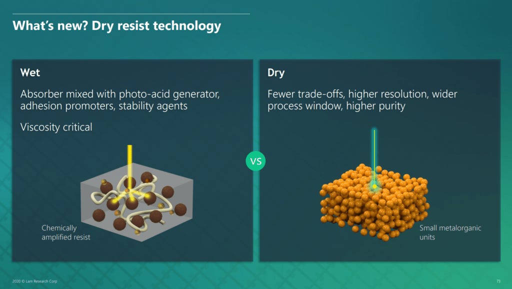
There is a battle brewing in the photoresist, coater, and developer market due to EUV advancement. This battle could cost Tokyo Electron their dominance over a $5B+ annual revenue market and lead to some photoresist companies such as TOK to lose a major market. JSR and Tokyo are bringing Metal Oxide Resist (MOR) to the market to fight off Lam Research's encroachment with their dry resist technology.

Combined, China and Taiwan would hold about 37% of global IC capacity, almost 3x that of North America. IC Industry at Heart of Possible China Takeover of Taiwan
[Twitter thread, Hacker News discussion]

Some things will get better from a design perspective, while others will be worse.

Gallium, once an industrial-waste product, is transforming our increasingly electrified world.

There are some features in any architecture that are essential, foundational, and non-negotiable. Right up to the moment that some clever architect shows
Intel is the poster child of how stock buybacks come at the cost of technological innovation.

Using yield analytics and consolidated data to power your factory.
Xoilac - Thiên đường bóng đá trực tuyến. Hãy cùng chúng tôi khám phá thêm về sự chuyên nghiệp và tận tâm trong dịch vụ chăm sóc khách hàng mà trang mang lại!

Let’s Build a Chip – We lay out the costs of building a chip – with spreadsheets!

Like its U.S. counterpart, Google, Baidu has made significant investments to build robust, large-scale systems to support global advertising programs. As

Its second analog AI chip is optimized for different card sizes, but still aimed at computer vision workloads at the edge.

Current custom AI hardware devices are built around super-efficient, high performance matrix multiplication. This category of accelerators includes the
New interconnects offer speed improvements, but tradeoffs include higher cost, complexity, and new manufacturing challenges.

AMD recently unveiled 3D V-Cache, their first 3D-stacked technology-based product. Leapfrogging contemporary 3D bonding technologies, AMD jumped directly into advanced packaging with direct bonding and an order of magnitude higher wire density.
Although competition from Arm is increasing, AMD remains Intel’s biggest competitor, as concerns of losing market share weigh on Intel’s valuation.

A full fix for the “Half-Double” technique will require rethinking how memory semiconductors are designed.

A new CPU design has won accolades for defeating the hacking efforts of nearly 600 experts during a DARPA challenge. Its approach could help us close side-channel vulnerabilities in the future.

Google detailed TPUv4 at Google I/O 2021. They're accelerator chips that deliver high performance on AI workloads.

Modern analog computers offer unique programming challenges which make them challenging compilation targets. How do we automatically program an analog computer to implement a computation?
.png)
The 2021 Perception Sensor Industry Map: Depth Sensing, LiDAR, CMOS, IMU, Software and More.

Presented by Robert Beachler, VP of Product, Untether AI. Traditional processor architectures are failing to keep up with the exploding compute demands of AI workloads. They are limited by the power-hungry weight-fetch of von Neumann architectures and limitations of transistor and frequency scaling. At-memory computation places compute elements directly in the memory array, providing reduced power consumption and increased throughput due to the massive parallelism and bandwidth provided by the architecture. This presentation introduces a new class of non-von Neumann compute designed to meet these AI demands. The Linley Fall Processor Conference featured technical presentations addressing processors and IP cores for AI applications, embedded, data center, automotive, and communications. Session topic included AI in Edge Devices, Vector-Processing Cores, Advancing Cloud AI, The New Infrastructure Edge, Heterogenous Computing, SoC Design, In-Memory Compute, and Security. Proceedings from the event are available for download. https://www.linleygroup.com/events/proc_register.php?num=49

Pushing AI to the edge requires new architectures, tools, and approaches.

Decisions that affect how, when, and where data gets processed.

Apple is positioning its M1 quite differently from any CPU Intel or AMD has released. The long-term impact on the PC market could be significant.

Sapphire Rapids, Intel's next server architecture, looks like a large leap over the just-launched Ice Lake SP.
BLOOMINGTON, Minn. and SAN JOSE, Calif. – April 6, 2021 – SkyWater Technology, the trusted technology realization partner, and Efabless, a crowdsourcing design platform for custom silicon, today announced the first tapeout in a series of Google-sponsored open source multi-project wafer (MPW) shuttles, managed by Efabless and manufactured at SkyWater. In this partnership, open source designs were selected to
What makes a GPU a GPU, and when did we start calling it that? Turns out that’s a more complicated question than it sounds.

How much should one pay for a chip or a component? Lytica, a Canadian supply-chain pricing analytics company, has the answer. Founded by former Nortel chief procurement officer Ken Bradley, who, like many others in the IT industry, was once bemused by component pricing, Lytica is transforming itself into a software-as-a-service (SaaS) company, helping OEM and EMS make well-informed deals when buying or selling.
The “Milan” Epyc 7003 processors, the third generation of AMD’s revitalized server CPUs, is now in the field, and we await the entry of the “Ice Lake”

AMD is one of the oldest designers of large scale microprocessors and has been the subject of polarizing debate among technology enthusiasts for nearly 50 years. Its...
SRAM cell architecture introduction: design and process challenges assessment.
One of the main tenets of the hyperscalers and cloud builders is that they buy what they can and they only build what they must. And if they are building
AMD ROCm documentation
With every passing year, as AMD first talked about its plans to re-enter the server processor arena and give Intel some real, much needed, and very direct

Here's what we've learnt about networks and the routers that interconnect them in the last 50 years.
We have a bad case of the silicon shakes and a worsening deficiency in iron here at The Next Platform, but the good news is that new CPU processors from

The breakthrough is taking full advantage of the orbital angular momentum properties of a coherent light source, thus enabling multiplexing.

Despite high development costs, smaller nodes bring greater revenue per wafer.

IC Insights recently released its new Global Wafer Capacity 2021-2025 report that provides details, analyses, and forecasts for IC industry capacity by wafer size, process geometry, region, and product type through 2025. Rankings of IC manufacturers by installed capacity for each of the wafer sizes are shown in Figure 1. The chart also compares the relative

The inception of Google’s effort to build its own AI chips is quite well known by now but in the interests of review, we’ll note that as early 2013 the

The hardware shortages currently hitting most of the PC market may be caused by a shortage in a necessary component in chip manufacturing, not low yields on TSMC's 7nm node.

How Compute Express Link provides a means of connecting a wide range of heterogeneous computing elements.
Consumer electronics markets, the mobile phone market in particular, are extremely demanding. They are driven by the desire to pack more and more functionality and enhanced value into the same size handheld device, and often at lower costs. This drive towards smaller, cheaper and thinner consumer electronics has driven the development of highly integrated electronics
Flexible Tape-and-Reel Circuit Substrate, High-end FPC, tape-and-reel, FPC, COF film, tape, single-piece packaging, Circuit Substrate,COF tape, tape film, substrate
Understanding Intel® processor names and numbers helps identify the best laptop, desktop, or mobile device CPU for your computing needs.
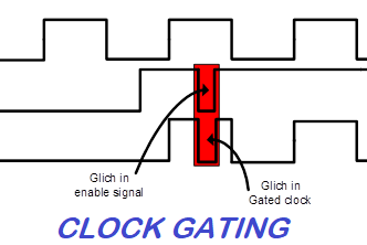
Clock Gating is defined as: “Clock gating is a technique/methodology to turn off the clock to certain parts of the digital design when not needed”. The Need for Clock Gating With most of the SoCs heavily constrained by power budgets, it is of utmost importance to reduce power consumption as much as possible

Leakage current can contribute to power dissipation, especially at lower threshold voltages. Learn about six types of leakage current that can be found in MOS transistors.

In this series of articles, we’ll explore higher-output-current alternatives to photodiodes.
Gate-all-around FETs will replace finFETs, but the transition will be costly and difficult.

Intel is in much more danger than its profits suggest; the problems are a long time in the making, and the solution is to split up the company.

How can you calculate the number of dies per wafer? A free online tool, DPW equation and reference to two other DPW calculators. Trusted by Amkor and GF.
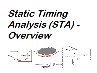
Static Timing Analysis? Read here the best overview to STA, including theory, real examples, ilustrations, tips and tricks.

In this article, we’ll discuss another group of thermal data, called thermal characterization parameters denoted by the Greek letter Psi (Ψ).

DIE YIELD CALCULATOR Use this online calculator to figure out die yield using Murphy’s model. You’ll need to know the die size, wafer diameter, and defect density. iSine is your complete resource for ASIC design – from concept to manufacturing and testing. We have expertise in system architecture, VHDL, Verilog, gate arrays, mixed signal, full...

Long-time Slashdot reader UnknowingFool writes: AMD filed a patent on using chiplets for a GPU with hints on why it has waited this long to extend their CPU strategy to GPUs. The latency between chiplets poses more of a performance problem for GPUs, and AMD is attempting to solve the problem with a ...

Learn about an important thermal metric for designing the interface between an IC package and a heat sink.

Watch the thermal measurement, junction-to-case thermal resistance, in action as we use it to calculate the thermal considerations for a given system.
Intel has been talking about on-processor FPGAs since 2014, but AMD's patent might actually result in one.

Research on 2D transistors for future electronics is forging ahead with different material favorites

Engineers must keep pace with advanced IC packaging technology as it evolves rapidly, starting with understanding the basic terms.

In the last part of our series, we went over the thin-film process in which a semiconductor chip gets its electrical properties. But we need to ensure that

Assessing the thermal performance of an IC package becomes easier if you understand this common, but often misapplied, parameter known as theta JA.

With 5G rolling out more quickly as we approach 2021, it may be helpful to touch on the key technologies that make 5G such a speedy success.

In this article, we will learn how to find the optimal size of a transistor/logic gate present in a larger circuit to provide the desired performance using the linear delay model.
This is a list of semiconductor fabrication plants. A semiconductor fabrication plant is where integrated circuits (ICs), also known as microchips, are manufactured. They are either operated by Integrated Device Manufacturers (IDMs) that design and manufacture ICs in-house and may also manufacture designs from design-only (fabless firms), or by pure play foundries that manufacture designs from fabless companies and do not design their own ICs. Some pure play foundries like TSMC offer IC design services, and others, like Samsung, design and manufacture ICs for customers, while also designing, manufacturing and selling their own ICs.

As implementations evolve to stay relevant, a new technology threatens to overtake SerDes.

How side-band, inline, on-die, and link error correcting schemes work and the applications to which they are best suited.
The most obvious question here is “why do I need…

Can we detect bugs in post- and pre-silicon testing where…

The parts that make up a complete and fully compatible STDF or ATDF file.

The IC industry is renewing its focus on advanced packaging. Chiplets may be the least mature option, but it is also one of the most widely promising. A conversation with Intel's Ramune Nagisetty.

How an integrated chip–package co-analysis can quickly and accurately model package layout for inclusion in on-chip power integrity simulations.

Taiwanese chip titan testing new production tech to boost computing power

The Computer Express Link interconnect builds on PCI Express 5.0 to enable memory coherency and low latency between host processors and accelerators.
When they were first commercialized at the 22 nm node, finFETs represented a revolutionary change to the way we build transistors, the tiny switches in the “brains” of a chip. As compared to...

In this article, we'll discuss the Elmore delay model, which provides a simplistic delay analysis that avoids time-consuming numerical integration/differential equations of an RC network.
We have nothing against disk drives. Seriously. And in fact, we are amazed at the amount of innovation that continues to go into the last

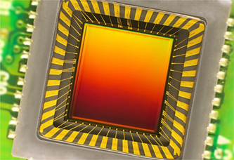
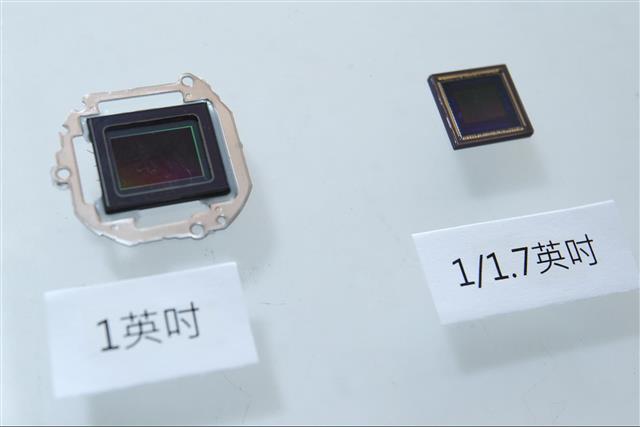
In this article, you'll learn the basics of the CMOS image sensor, including its core components, its block diagram, its strengths and weaknesses, and its applications.
But so are better approaches to deal with thorny counterfeiting issues.
The semiconductor industry growth is increasing exponentially with high speed…
Looking at a typical SoC design today it's likely to…

Adoption of new format will take time, but it also will add consistency into data as volume grows.
In this article, I would like to shortly describe the methods used to dump and restore the different kinds of registers on 32-bit and 64-bit x86 CPUs. The first part will focus on General Purpose Registers, Debug Registers and Floating-Point Registers up to the XMM registers provided by the SSE extension. I will explain how their values can be obtained via the ptrace(2) interface.

A different approach to speeding up AI and improving efficiency.

With no definitive release date for DDR5, DDR4 is making significant strides.

They say "performance is king'... It was true a decade ago and it certainly is now. With more and mor...

Single-clock design is not always as easy as it seems.
More about the data that the fab makes available to the fabless customer when the wafer is ready to ship.

The principle of shielding is creating a conductive layer completely surrounding the object you want to shield. This was invented by Michael Faraday and this system is known as a Faraday cage.

As next-gen data centers amp up processing and speed, they're going to need processing units that can handle the heft of AI and machine learning.

In this article, we will review the different types of noise that are present in a circuit. We will also discuss how to perform an accurate simulation of an EMC filter with LTspice.

Nvidia tops MLPerf records again, consortium adds benchmarks to measure mobile
This is the official source code of FreeCAD, a free and opensource multiplatform 3D parametric modeler. - FreeCAD/FreeCAD
While the Intel Extreme Tuning Utility (XTU) on Windows allows for undervolting laptop processors, currently on Linux there isn't any Intel-endorsed way for undervolting your CPU should you be interested in better thermal/power efficiency and other factors

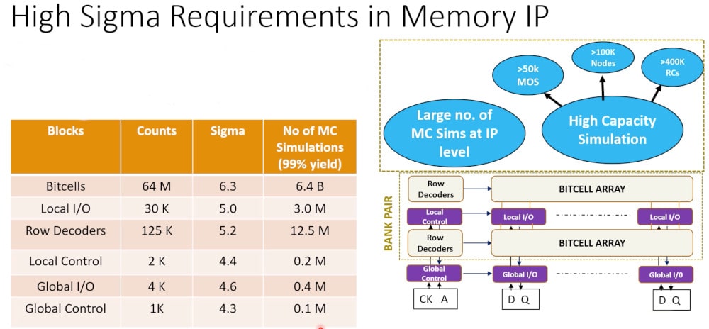
Variation-aware memory verification with brute force Monte Carlo accuracy in much less time.
What is the hardest job at Intel, excepting whoever is in charge of the development of chip etching processes and the foundries that implement it? We
Designed for your current needs and future ambitions, Marvell delivers the data infrastructure technology transforming tomorrow’s enterprise, cloud, automotive, and carrier architectures for the better.

Micron's GDDR6X is one of the star components in Nvidia's RTX 3070, 3080, and 3080 video cards. It's so fast it should boost gaming past the 4K barrier.

Qualcomm says mmWave could get better soon, as it's completed a test that doubles the theoretical range of mmWave to 2.36 miles (3.8 kilometers).
[Jean-Francois Debroux] spent 35 years designing analog ASICs. He’s started a book and while it isn’t finished — indeed he says it may never be — the 180 pages he posted on …
China-based DRAM chipmaker ChangXin Memory Technologies (CXMT) is scaling up its 19nm chip output with better yield rates, with the monthly production likely to top 70,000 wafers by the end of 2020, according to industry sources.

Ahead of the Hot Chips 2020 conference this week, photonics chip startup Lightmatter detailed its forthcoming test chip accelerator hardware.

When it comes to hashing, sometimes 64 bit is not enough, for example, because of birthday paradox — the hacker can iterate through random $latex 2^{32}$ entities and it can be proven that wi…

Tim Ansell of Google has announced the open-source SkyWater PDK, and plans to manufacture 40 open-source SoC projects for free by 2021.

Hardware solutions that mitigate the design challenges and meet requirements of the latest tropospheric scatter applications.
In its Global Wafer Capacity 2020-2024 report, IC Insights breaks down the world’s installed monthly IC wafer capacity by geographic region (or country). Figure 1 shows the installed IC capacity by region as of December of 2019. To clarify what the data represents, each regional number is the total installed monthly capacity of fabs located in
Did you ever dream about creating your own physical chip? Do it today. For free. Fully open source.
The CORE-V CVA6 is an Application class 6-stage RISC-V CPU capable of booting Linux - openhwgroup/cva6
Open source process design kit for usage with SkyWater Technology Foundry's 130nm node. - google/skywater-pdk

In this article, we briefly review how the Laplace transform can help us solve circuits involving damped and steady-state sinusoidal signals.

This Frequent Engineering Question gives a quick overview of an important mathematical technique used in digital signal processing, calculating the z-transform.
The x86 instruction set refers to the set of instructions that x86-compatible microprocessors support. The instructions are usually part of an executable program, often stored as a computer file and executed on the processor.
Compute paradigm shifting as more data needs to be processed more quickly.

New transistors structures are on the horizon with new tools and processes, but there are lots of problems, too.

Discover 100 collaborative articles on domains such as Marketing, Public Administration, and Healthcare. Our expertly curated collection combines AI-generated content with insights and advice from industry experts, providing you with unique perspectives and up-to-date information on many skills and their applications.
When you have 54.2 billion transistors to play with, you can pack a lot of different functionality into a computing device, and this is precisely what
Qualcomm open sources the AI Model Efficiency Toolkit on GitHub, providing a simple library plugin for AI developers.
Fujitsu Limited today announced that it began shipping the supercomputer Fugaku, which is jointly developed with RIKEN and promoted by the Ministry of Education, Culture, Sports, Science and Technology with the aim of starting general operation between 2021 and 2022. The first machine to be shipped this time is one of the computer units of Fugaku, a supercomputer system comprised of over 150,000 high-performance CPUs connected together. Fujitsu will continue to deliver the units to RIKEN Center for Computational Science in Kobe, Japan, for installation and tuning.

Hybrid solutions emerging as reliability concerns increase and coverage becomes more difficult.

There's a new wave of counterfeit Intel CPUs popping up in China, and chips like the 7700K appear especially "popular" for re-use.
An intuitive tutorial of antennas and antenna theory. This website is designed to present a comprehensive overview of antennas, from design, to measurement and theory. Unnecessarily complicated math is avoided throughout.
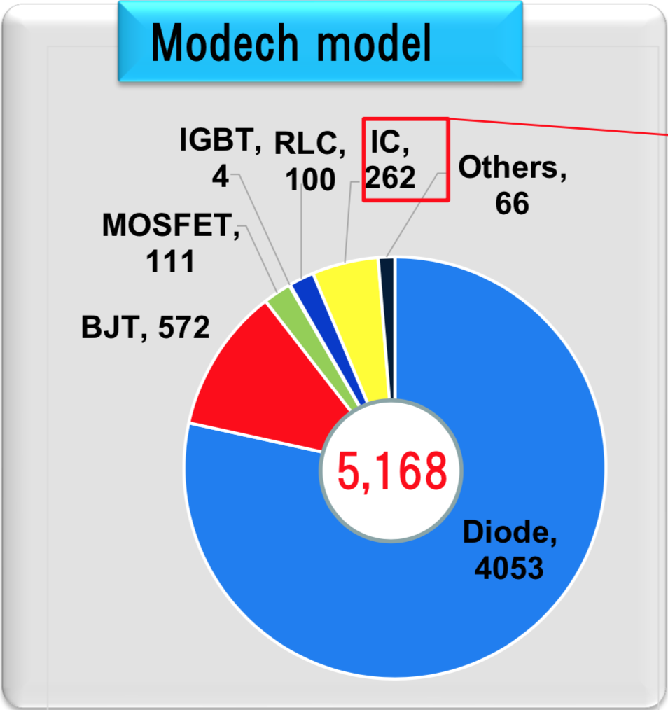
SPICE (Simulation Program with Integrated Circuit Emphasis) is an open-source analog electronic circuit simulator. | SPICE is undoubtedly one of the most popular modeling libraries available, and Japanese e-commerce company MoDeCH is seeking to make the power of SPICE available to everyone.

This article, the first in a series, discusses light-sensitive electronic devices called photodiodes and compares CCD and CMOS sensors.
TSMC details its 5-nanometer node for mobile and HPC applications. The process features the industry's highest density transistors with a high-mobility channel and highest-density SRAM cells.

Learn the basics of the ultra-wideband short-range wireless protocol, a technology that can be found in cutting-edge devices.
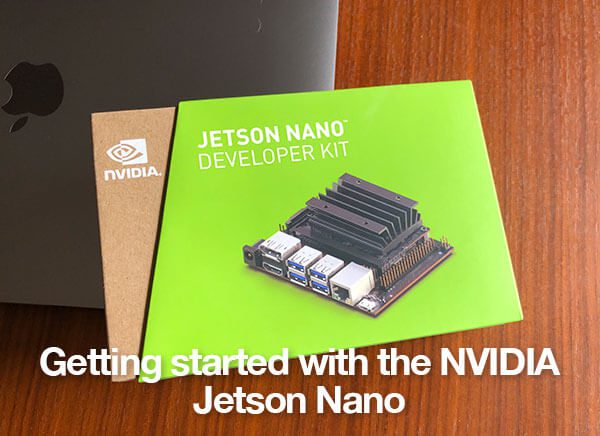
In this tutorial, you will learn how to get started with your NVIDIA Jetson Nano, including installing Keras + TensorFlow, accessing the camera, and performing image classification and object detection.

Learn how to get faster composite op-amp dynamics by raising the slew rate.

The latest banks and financial services company and industry news with expert analysis from the BBVA, Banco Bilbao Vizcaya Argentaria.
The success and proliferation of integrated circuits has largely hinged on the ability of IC manufacturers to continue offering more performance and functionality for the money. Driving down the cost of ICs (on a per-function or per-performance basis) is inescapably tied to a growing arsenal of technologies and wafer-fab manufacturing disciplines as mainstream CMOS processes
Recently, I’ve started to explore RISC-V. I experienced the journey as pretty refreshing, particularly because I’ve been working on x86 low-level software almost exclusively for about 10 years.
Previously, as they used to say at the start of a new episode in a TV series, we discussed the history behind the use of hardware vs. software to debounce our switches. We also perused and pondered…
At DesignCon 2020, ANSYS sponsored a series of very high-quality…
OmniVision Technologies has announced at CES 2020 the OV48C, a 48 megapixel (MP) image sensor with a large 1.2 micron pixel size to enable high resolution and low light performance for flagship smartphone cameras.

The authoritative information platform to the semiconductor industry.
The Silvaco Technical Library includes Application Notes, issues of the Simulation Standard Journal, Presentations, Published Papers, and Whitepapers.
A look at Cerebras Wafer-Scale Engine (WSE), a chip the size of a wafer, packing over 400K tiny AI cores using 1.2 trillion transistors on a half square foot of silicon.
363 votes, 25 comments. This post has been split into a two-part series to work around Reddit’s per-post character limit. Please find Part 2 in the…

Good inferencing chips can move data very quickly
Making sure IO rings comply with IP and SoC design rules.

Runaway complexity is making it more difficult and critical to deal with signal integrity in a system context.

Recent leaks may shed some light on Intel's upcoming mainstream desktop Comet Lake-S CPUs.
A dizzying array of choices and options pave the way for the next phase of scaling.

Intel's Tremont CPU microarchitecture will be the foundation of a next-generation, low-power processors that target a wide variety of products across
A post describing how C programs get to the main function. Devicetree layouts, linker scripts, minimal C runtimes, GDB and QEMU, basic RISC-V assembly, and other topics are reviewed along the way.

“Industry 4.0” is already here for some companies—especially silicon foundries.
An update on TSMC current and forthcoming logic process nodes as well as their next-generation advanced packaging technologies.

Michigan team builds memristors atop standard CMOS logic to demo a system that can do a variety of edge computing AI tasks

Areanna claims that a custom SRAM delivers 100 TOPS/W on deep learning, but it’s early days for the startup.
“The Google of the Semiconductor Industry” Founded in 2011, AnySilicon is the best way to explore, find and contact semiconductor service providers and IP vendors online. Our vision is to be the first place ASIC engineers and decision makers go to search for semiconductor service providers and IP core vendors. In addition to
Excessive instruction cache misses are the kind of a performance problem that's going to appear only in larger codebases. In this article, I'm describing some ideas on how to deal with this issue.

Boston-based startup Lightelligence's optical machine learning accelerator has entered prototyping stage, the startup announced.

Comparing different machine learning use-cases and the architectures being used to address them.

Optalysys, a startup based in the United Kingdom, has introduced an entry-level optical coprocessor, the first such system of its kind on the market. The

DigiKey offers a complete set of APIs to share information and automate the ordering process.
Repository for the tools and non-commercial data used for the "Accelerator wall" paper. - PrincetonUniversity/accelerator-wall
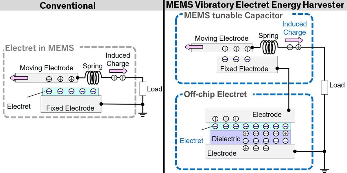
Scientists in Japan have developed a MEMS energy harvester charged by an off-chip electret
How the wrong benchmark can lead to incorrect conclusions.

Get a primer on the basics of supercapacitors, their functionality, and which applications they're best for.
Monday night Amazon announced the new 'A1' instance type for the Elastic Compute Cloud (EC2) that is powered by their own 'Graviton' ARMv8 processors.

It might have been difficult to see this happening a mere few years ago, but the National Nuclear Security Administration and one of its key

Accurately determine parasitic effects with the proper set up of two different methods.
A new metric can help companies pinpoint performance issues on the semiconductor supply chain.

The previous post in this series (excerpted from the Objective Analysis and Coughlin Associates Emerging Memory report) explained why emerging memories are necessary. Oddly enough, this series will explain bit selectors before defining all of the emerging memory technologies themselves. The reason why is that the bit selector determines how small a bit cell can

Why Chips Die Semiconductor devices face many hazards before and after manufacturing that can cause them to fail prematurely.
The average revenue generated from processed wafers among the four biggest pure-play foundries (TSMC, GlobalFoundries, UMC, and SMIC) is expected to be $1,138 in 2018, when expressed in 200mm-equivalent wafers, which is essentially flat from $1,136 in 2017, according to a new analysis by IC Insights (Figure 1). The average revenue per wafer among the

Process Corner Explosion, At 7nm and below, modeling what will actually show up in silicon is a lot more complicated.
Understanding aging factors within a design can help reduce the likelihood of product failures.

Processing In Memory Growing volume of data and limited improvements in performance create new opportunities for approaches that never got off the ground.

Wafer fabs are the backbone of every electronic product. Every chip consists of a piece of silicon that is produced in a wafer fab. Wafer fabs play a key role in the customer, medical and automotive markets because the are they enabler of innovative technologies. There are many wafer fabs globally and they have

Explore what’s new, what’s next, and what should be on your radar in the world of transportation. Our insights are supported by real-world data from our partners across the globe.

Micron notes that GDDR6 has silicon changes, channel enhancements, and talks a bit about performance measurements of the new memory.
Alchip Minimizes Dynamic Power for High-Performance Computing ASICs How a fabless chipmaker successfully reduced power consumption within its fishbone clock tree methodology.
Google did its best to impress this week at its annual IO conference. While Google rolled out a bunch of benchmarks that were run on its current Cloud TPU

Google's new TPUs are here -- and they're quite a bit faster than last year's model.

This article will review the structure of the binary multipliers that use the look-up tables (LUTs) in the Xilinx logic fabric.

Low power wireless technologies are adapting to the Internet of Things by including IP connectivity and mesh networking.

The multitude of short-range wireless technologies provides engineers with optimized solutions for their applications, but makes careful selection paramount.

New computing architectures aim to extend artificial intelligence from the cloud to smartphones

Imperfect Silicon, Near-Perfect Security Physically unclonable functions (PUF) seem tailor-made for IoT security.

If you were uncertain about the term “FlipChip” this tutorial will help you better understand what FlipChip packaging technology is all about. FlipChip package technology has been around for 3-4 decades and started as a package solution for high pin count & high performance package requirements. At the beginning, the majority of FlipChip
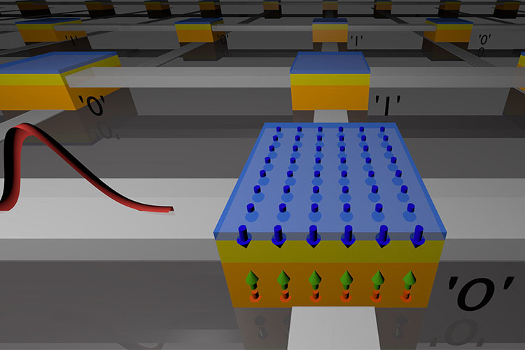
Breakthrough that could lead to greatly increased performance and more energy-efficient computer memory and processing technologies

With Mott memristors, a system could solve intractable problems using little power

Post date: Sep 19, 2014 10:01:08 PM

Making Waves in Deep Learning How deep learning applications will map onto a chip.
A new crop of applications is driving the market along some unexpected routes, in some cases bypassing the processor as the landmark for performance and
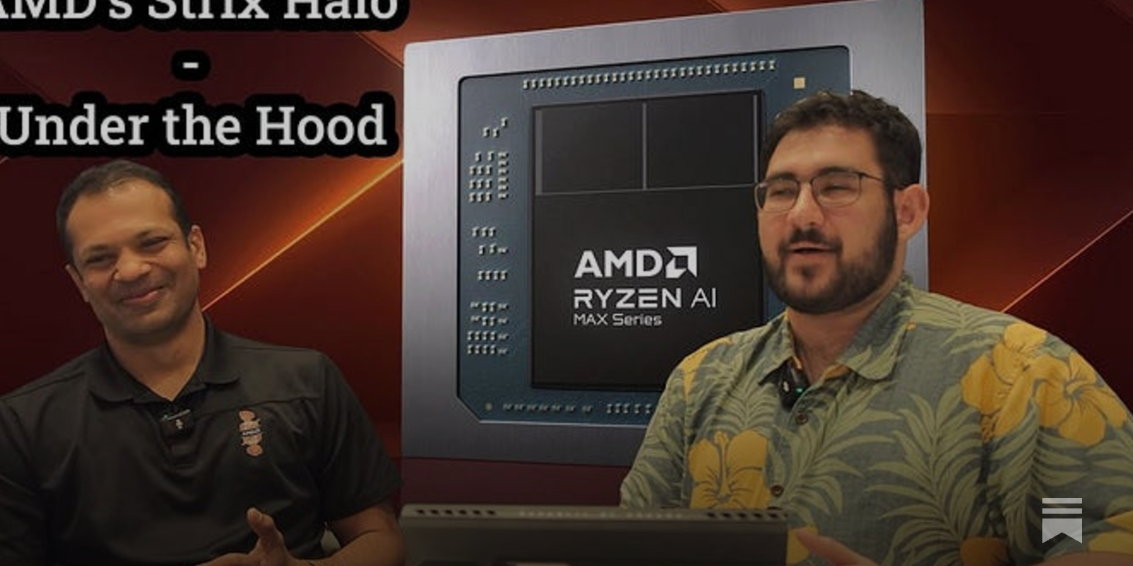


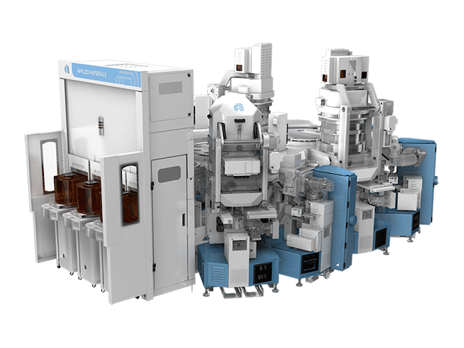
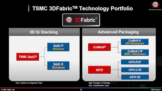
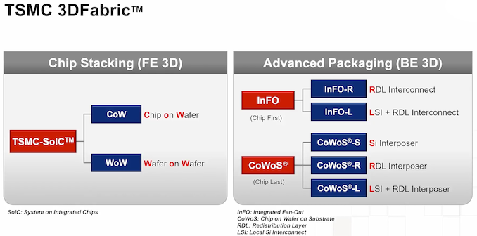


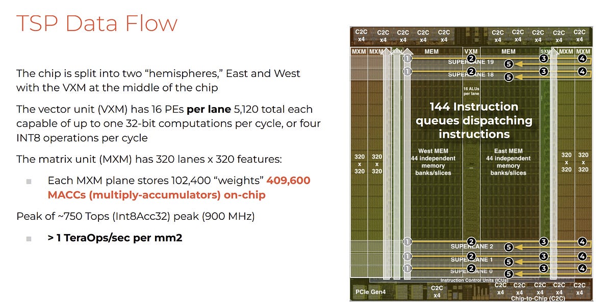
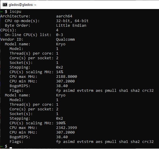


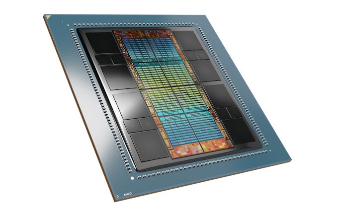

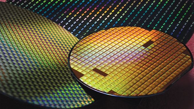
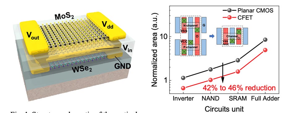
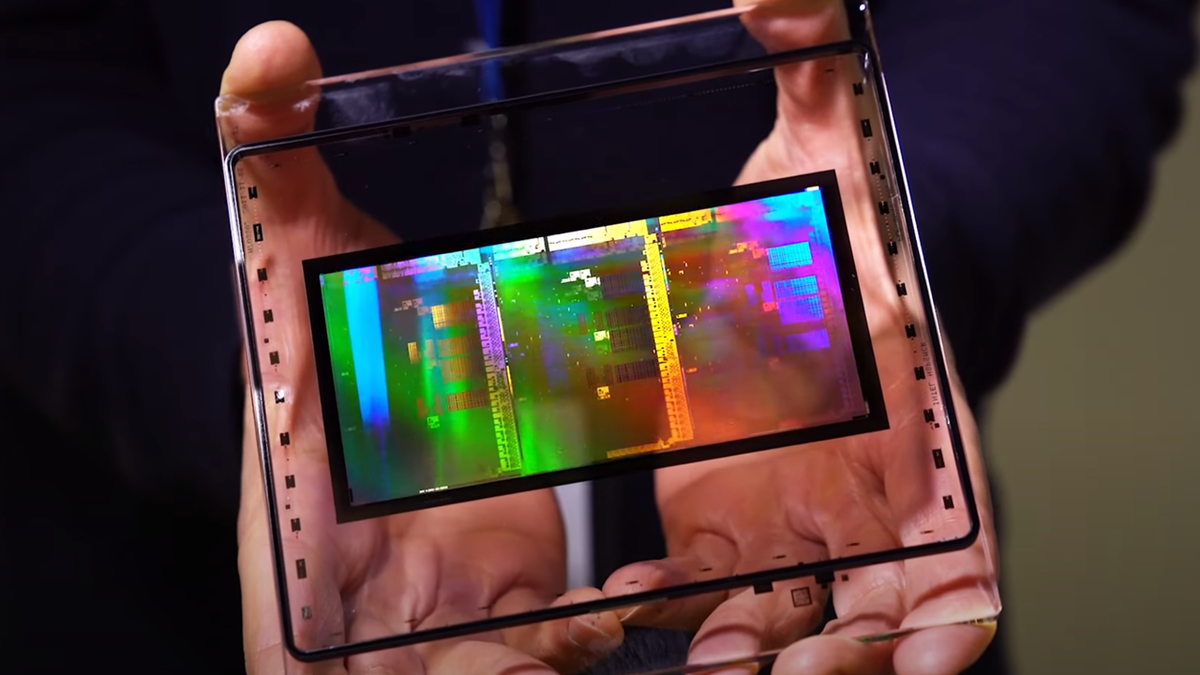


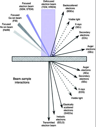
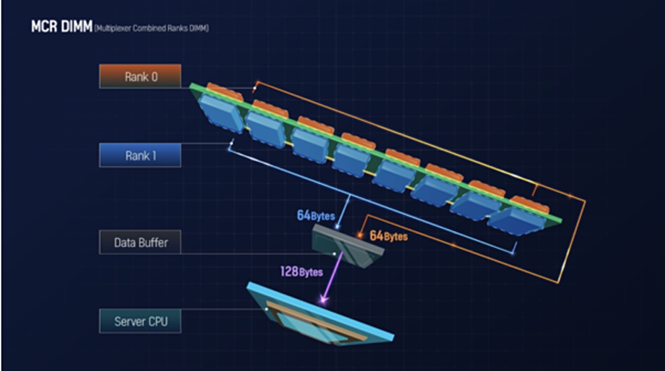

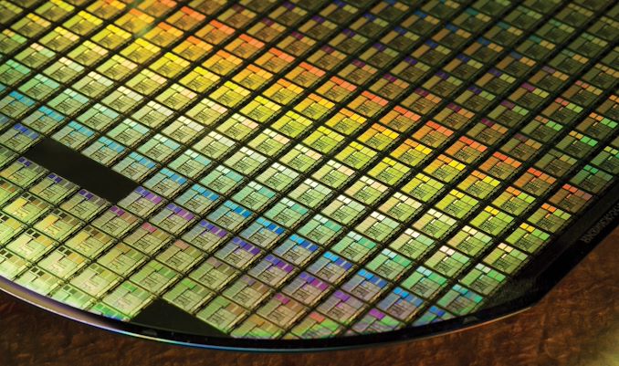
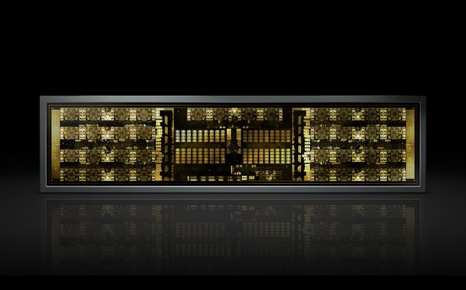
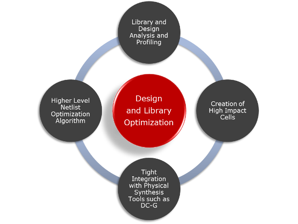
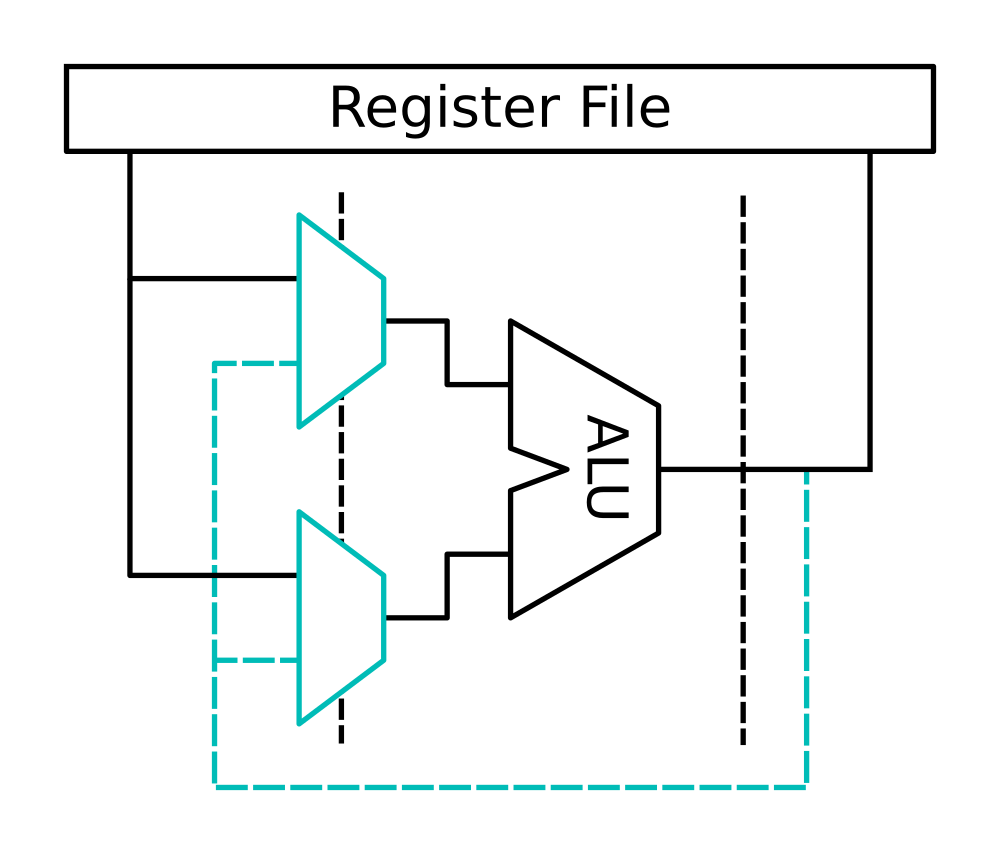

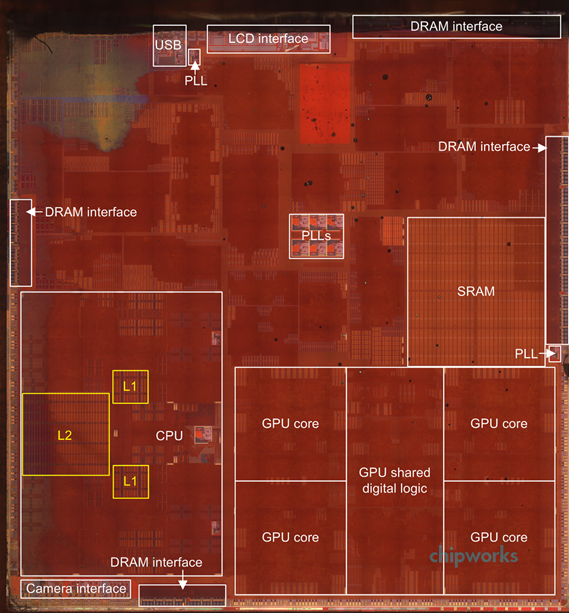
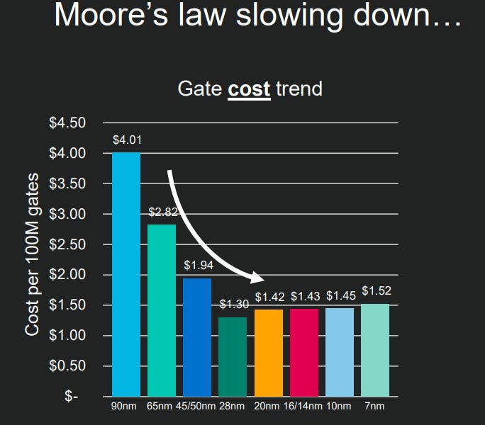
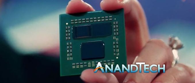
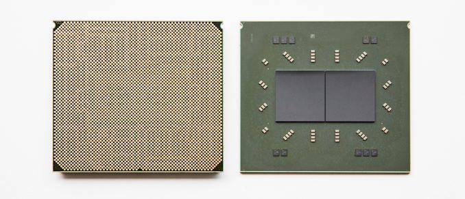
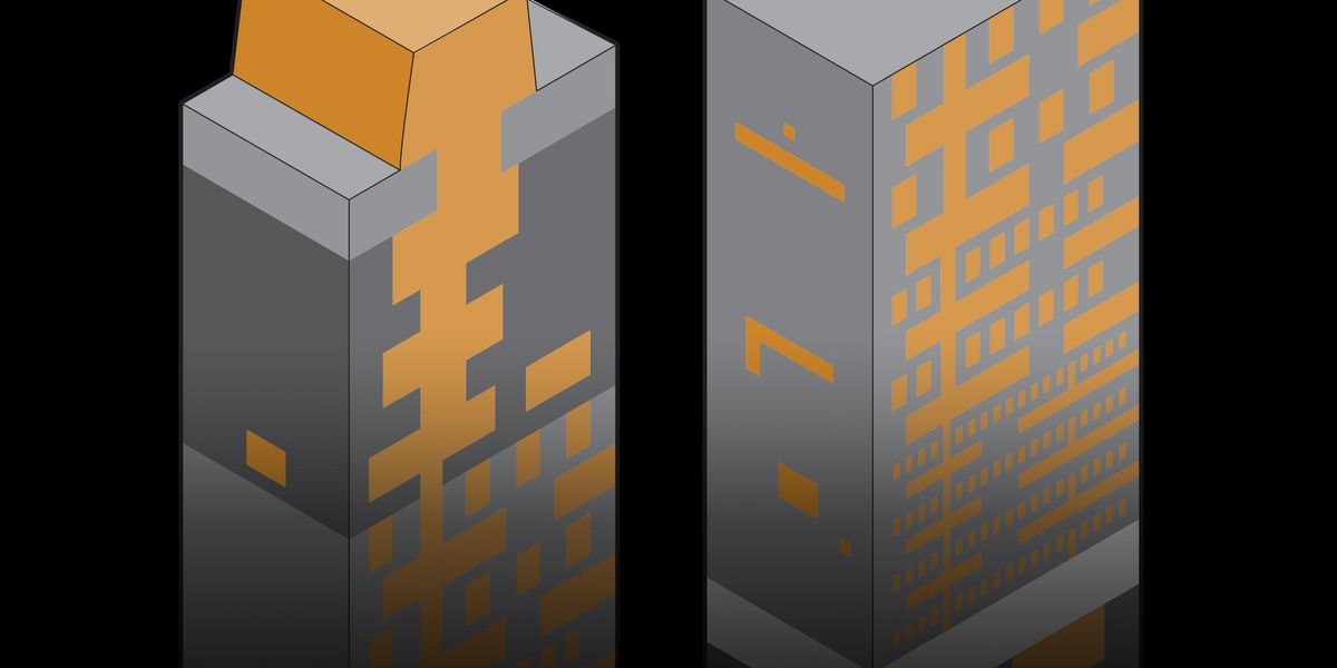

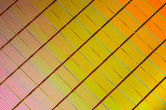


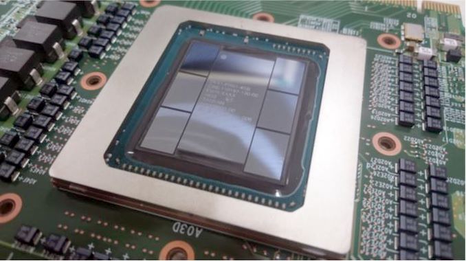

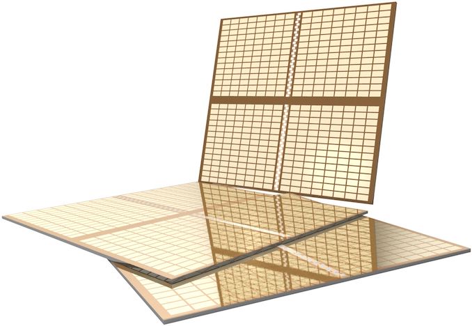
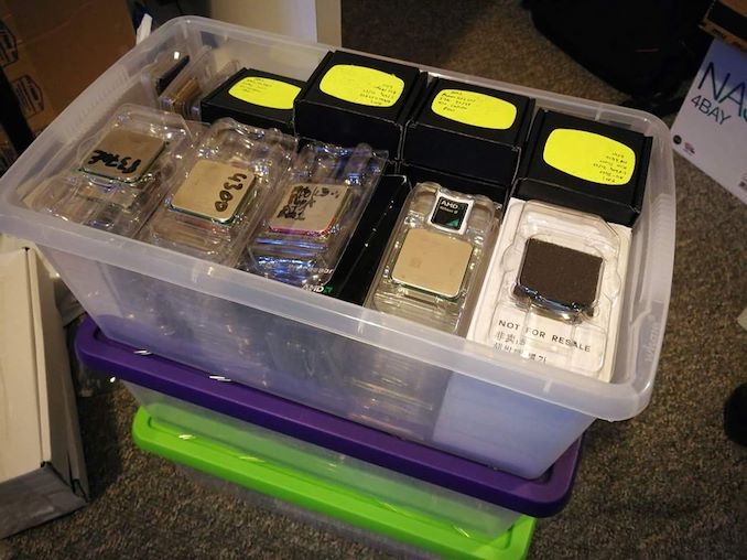
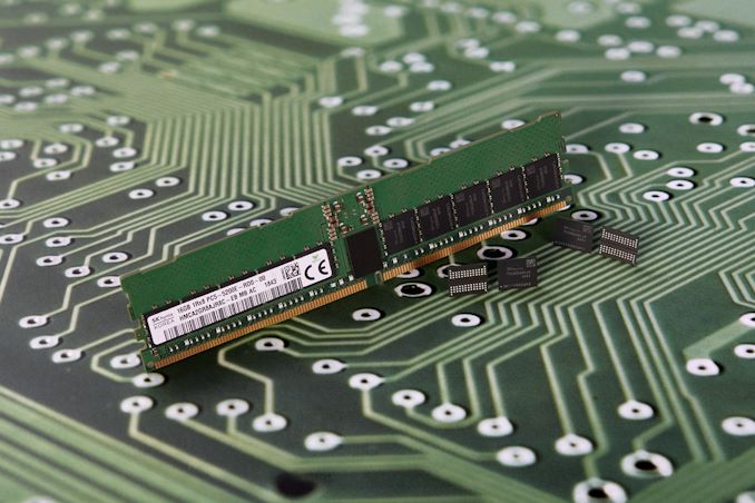

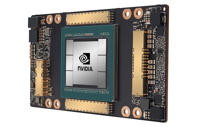
/cdn.vox-cdn.com/uploads/chorus_asset/file/12162773/akrales_180816_2793_0073.jpg)

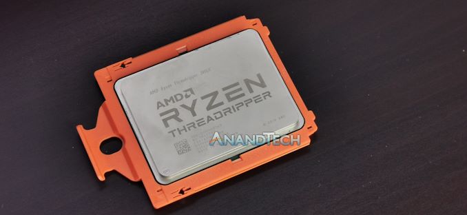

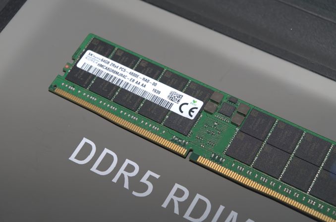
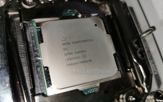
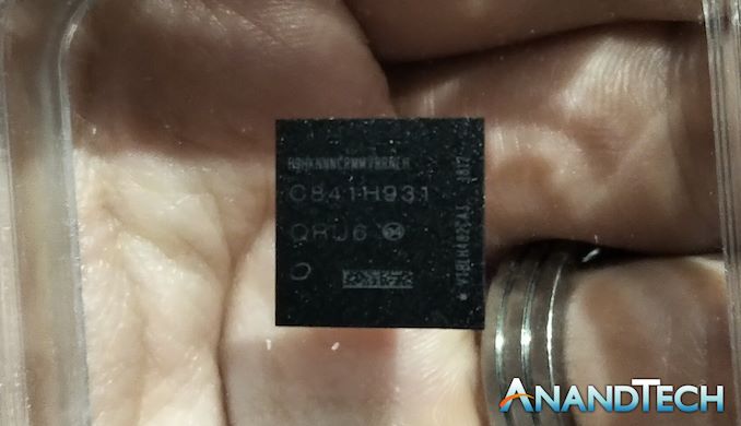


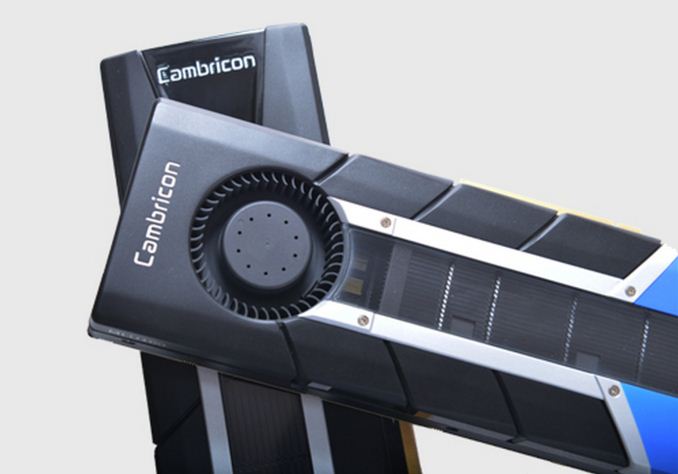
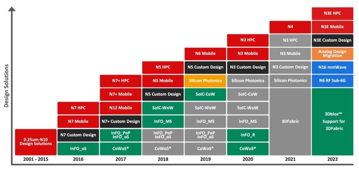