chip-design

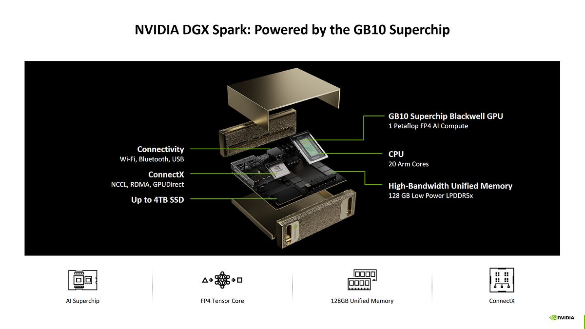
Looking at Nvidia's latest effort to make a big iGPU

Designing AI Chip Hardware and Software Bjarke Hammersholt Roune 2026 This document is, for now, open for comments. You can use the Google Docs comment feature to add comments anywhere. Thanks! What is this document? I was going to start an AI chip company and this document contains my thinking...

Taalas is replacing programmable GPUs with hardwired AI chips to achieve 17,000 tokens per second for ubiquitous inference

UC San Diego researchers have reimagined RRAM, creating a device that could redefine AI's memory challenges. Discover how this could impact edge computing.
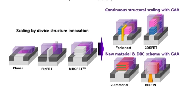
Key takeaways ▼ The transition from FinFET to Gate-All-Around (GAA) transistor technology represents a pivotal moment in the evolution of logic devices, driven by both physical scaling limits and the … Continue reading "Gate-All-Around (GAA) Technology for Sustainable AI"

In this article, we'll walk through the steps of generating a Process Design Kit (PDK) for digital standard cell libraries.

A new technical paper titled “Prefill vs. Decode Bottlenecks: SRAM-Frequency Tradeoffs and the Memory-Bandwidth Ceiling” was published by researchers at Uppsala University. Abstract “Energy consumption dictates the cost and environmental impact of deploying Large Language Models. This paper investigates the impact of on-chip SRAM size and operating frequency on the energy efficiency and performance of... » read more
Future AI Accelerators Might Need To Be Slower To Be Faster
FPGAs are limited by outdated proprietary software. Learn how embracing open-source tools is necessary to modernize FPGA development and unlock their full potential.

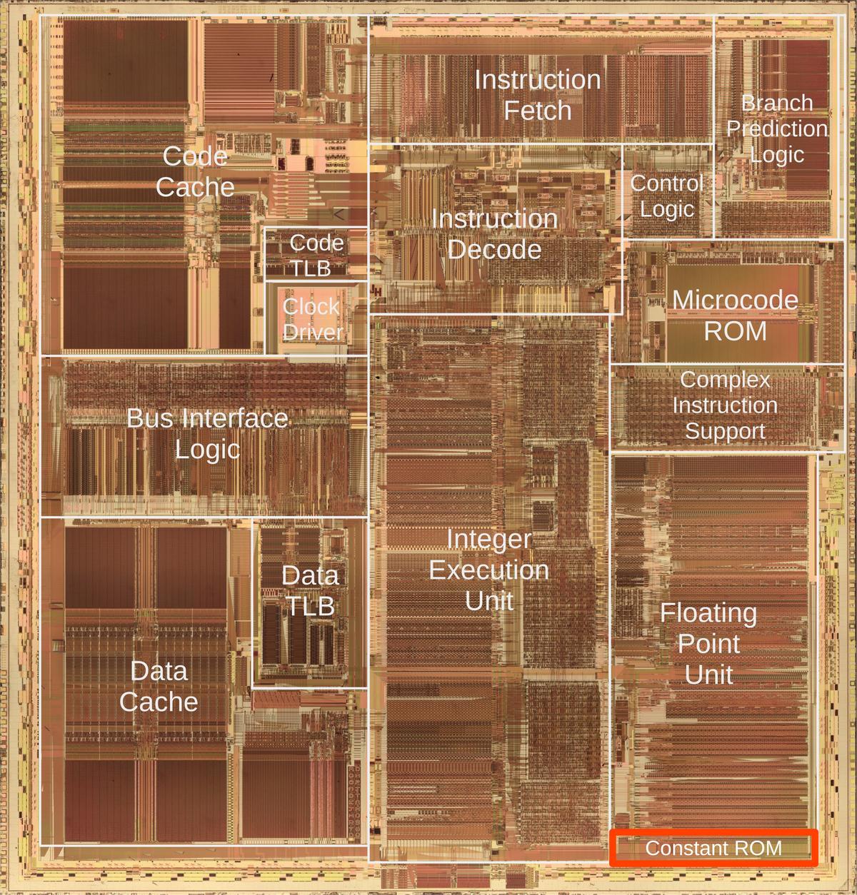
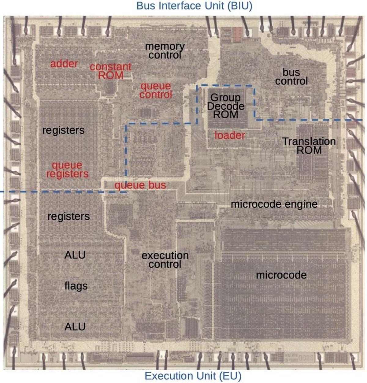
I've been studying the standard cell circuitry in the Intel 386 processor recently. The 386, introduced in 1985, was Intel's most complex pr...

Researchers focus on limiting data movement to reduce power and latency in edge devices.

Hello you fine Internet folks!

Bump technologies are being pushed beyond what was thought to be their physical and performance limits.

Motorola’s 68000 blended 32-bit power with a 16-bit bus, creating a balanced, orthogonal, and elegant architecture that powered everything from Macintosh to arcade machines.

Timing is increasingly dependent on vectors. Can static techniques continue to deliver the necessary results? Maybe.

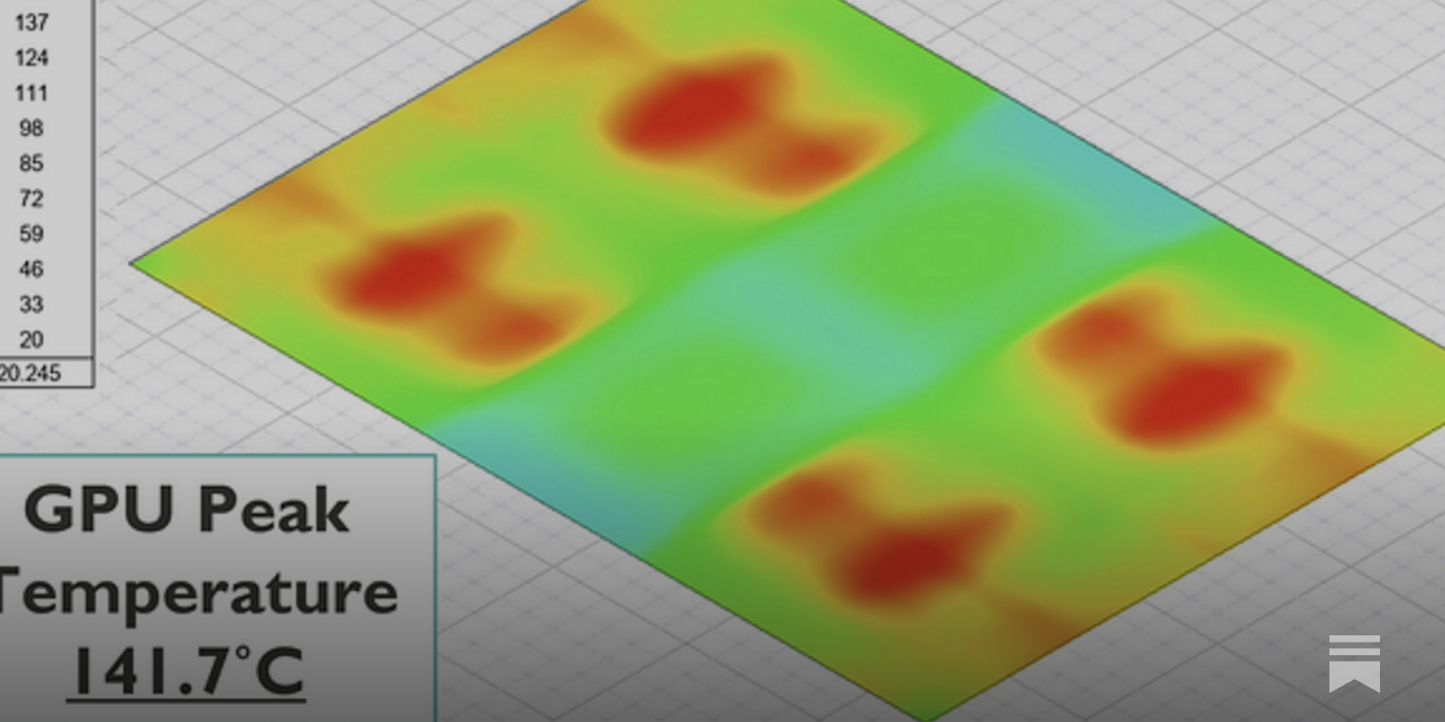
A new technical paper titled “On the Thermal Vulnerability of 3D-Stacked High-Bandwidth Memory Architectures” was published by researchers at North Carolina A&T State University and New Mexico State University. Abstract “3D-stacked High Bandwidth Memory (HBM) architectures provide high-performance memory interactions to address the well-known performance challenge, namely the memory wall. However, these architectures are susceptible... » read more
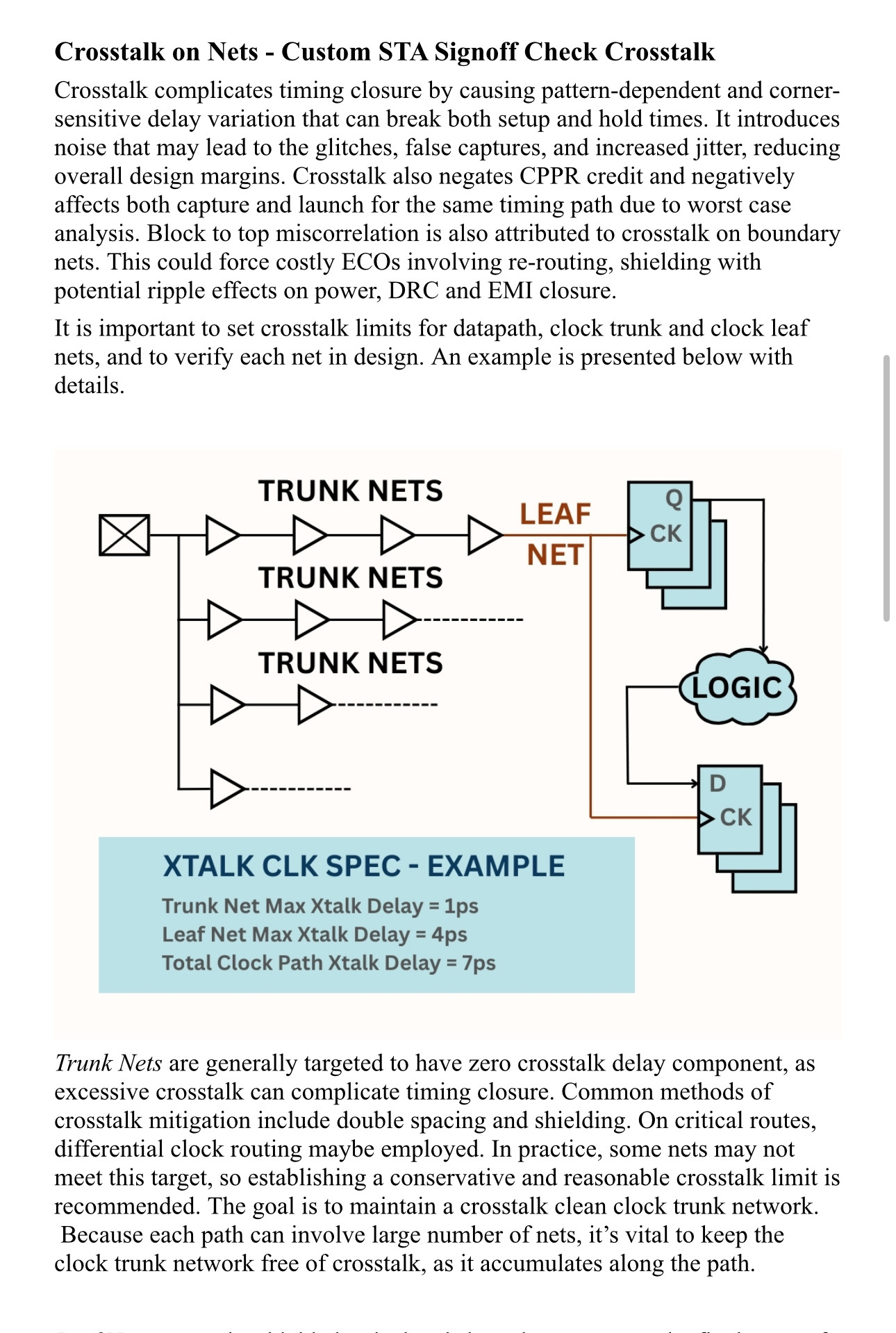
By Zameer Mohammed Once a chip is taped out, changes in design are not possible – Silicon is unforgiving, does not allow postproduction modifications. In contrast, software can be updated … Continue reading "Static Timing Analysis Signoff A comprehensive and Robust Approach"
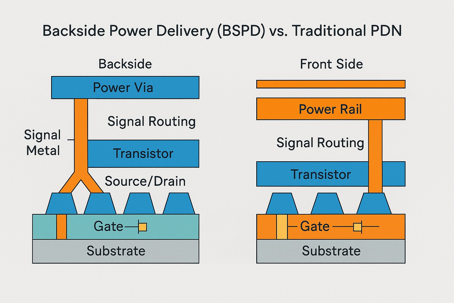
Backside Power Delivery (BSPD), also called Backside Power Delivery Network (BSPDN) or backside power via (BPV) technology, is a semiconductor manufacturing innovation in which the chip’s primary power distribution network … Continue reading "Backside Power Delivery (BSPD) Wiki"

Rapidus is advancing with its 2nm process. For the first time, the node's logic density has been reported, and it's on par with TSMC.

I've been reverse-engineering the Intel 386 processor (from 1985), and I've come across some interesting circuits for the chip's input/outpu...

Examining RDNA 4's out-of-order memory accesses in detail, and investigating with testing

Have you ever wanted to reverse engineer an analog chip from a die photo? Wanted to understand what's inside the "black box" of an integrate...

Finding defects now requires multiple data types, and a much more thorough search.
Thermodynamic computing isn't just a rebrand of probabilistic computing
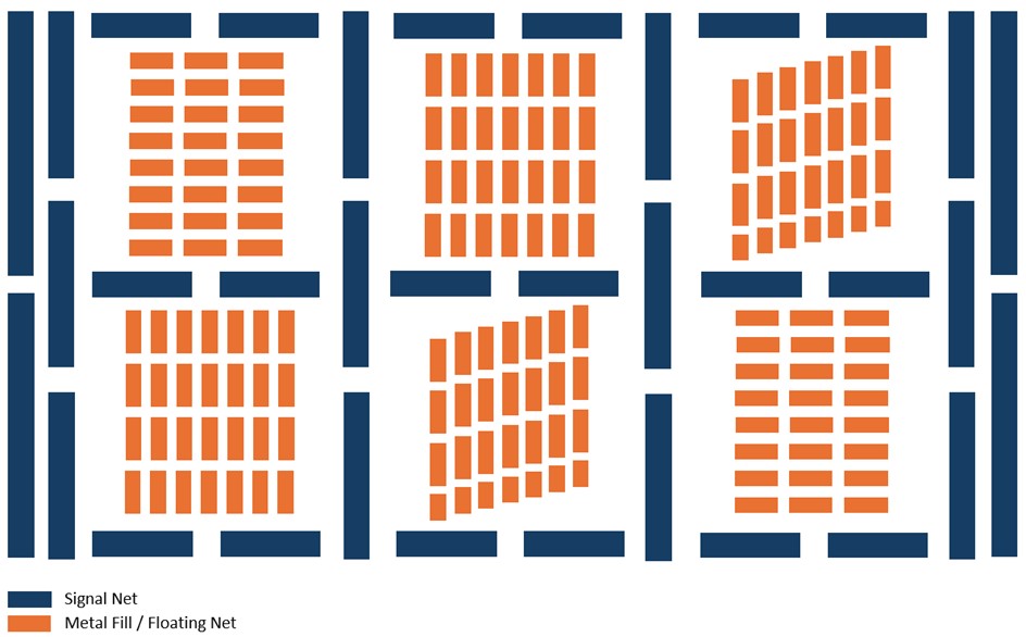
An adaptive metal fill extraction technique dynamically adjusts the level of detail based on the design context, such as the density of...

Many features of UCIe 2.0 seen as “heavy” are optional, causing confusion.


Most people think of machine instructions as the fundamental steps that a computer performs. However, many processors have another layer of ...
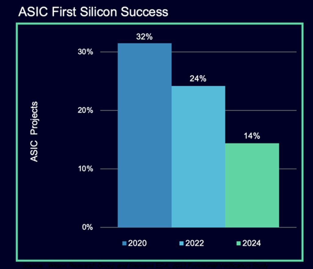
Number of designs that are late increases. Rapidly rising complexity is the leading cause, but tools, training, and workflows need to improve.
Hello you fine Internet folks,

In 1993, Intel released the high-performance Pentium processor, the start of the long-running Pentium line. I've been examining the Pentium'...

[vc_row][vc_column column_width_percent=”90″ gutter_size=”3″ overlay_alpha=”50″ shift_x=”0″ shift_y=”0″ shift_y_down=”0″ z_index=”0″ medium_width=”0″ mobile_width=”0″ width=”1/1″ uncode_shortcode_id=”158708″][vc_column_text uncode_shortcode_id=”154284″] Conventional wisdom in semiconductor manufacturing has long […]
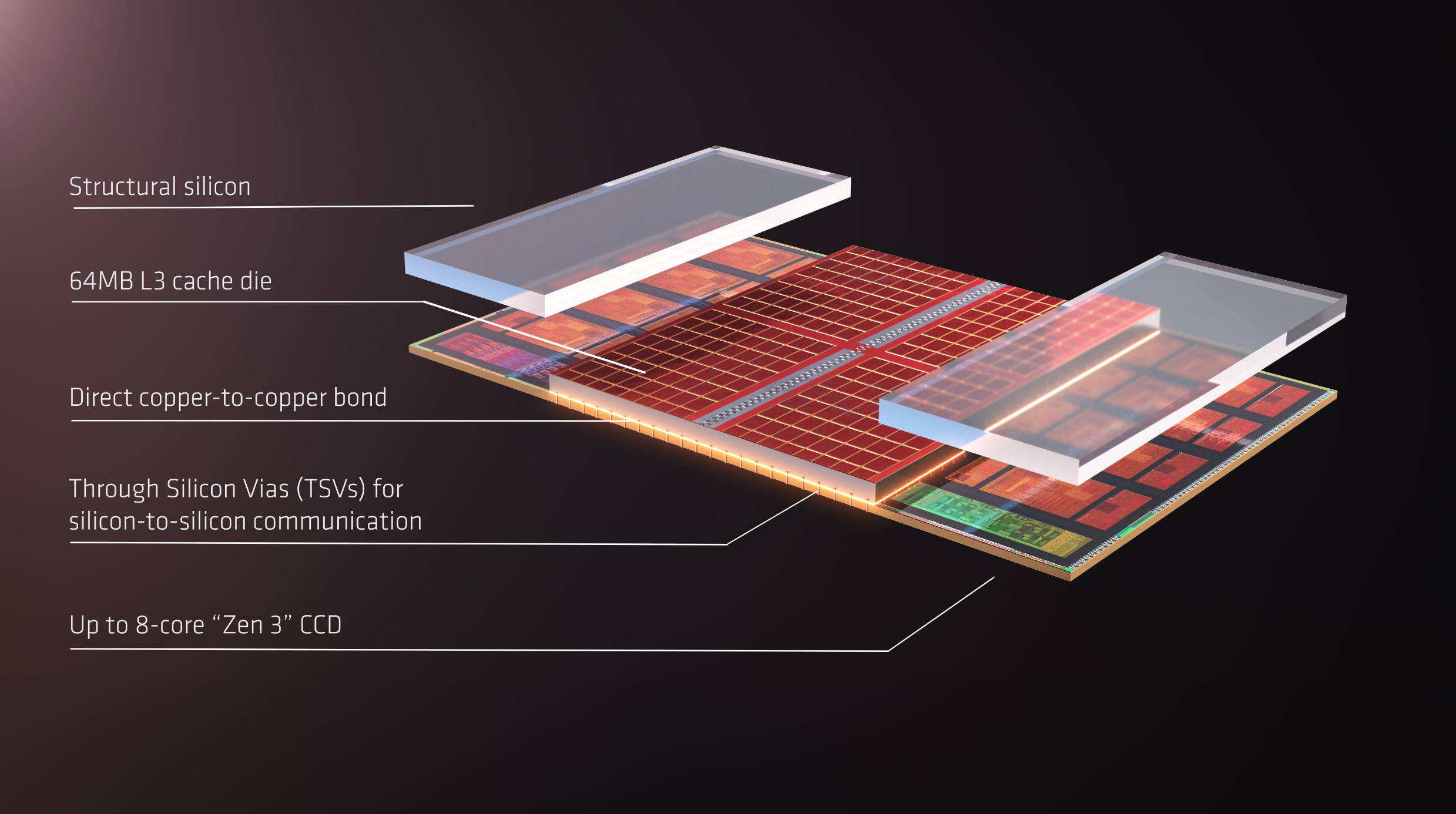
After persistent rumors refused to recede, AMD steps in with a clear explanation why dual-CCD V-Cache doesn't exist.
Intel released the powerful Pentium processor in 1993, establishing a long-running brand of high-performance processors. 1 The Pentium incl...

Designing neuromorphic sensory processing units (NSPUs) based on Temporal Neural Networks (TNNs) is a highly challenging task due to the reliance on manual, labor-intensive hardware development processes. TNNs have been identified as highly promising for real-time edge AI applications, mainly because they are energy-efficient and bio-inspired. However, available methodologies lack automation and are not very accessible. Consequently, the design process becomes complex, time-consuming, and requires specialized knowledge. It is through overcoming these challenges that one can unlock the full potential of TNNs for efficient and scalable processing of sensory signals. The current approaches to TNN development are fragmented workflows, as

In 1993, Intel released the high-performance Pentium processor, the start of the long-running Pentium line. The Pentium had many improvement...

Large Language Models (LLMs) have become a cornerstone of artificial intelligence, driving advancements in natural language processing and decision-making tasks. However, their extensive power demands, resulting from high computational overhead and frequent external memory access, significantly hinder their scalability and deployment, especially in energy-constrained environments such as edge devices. This escalates the cost of operation while also limiting accessibility to these LLMs, which therefore calls for energy-efficient approaches designed to handle billion-parameter models. Current approaches to reduce the computational and memory needs of LLMs are based either on general-purpose processors or on GPUs, with a combination of weight quantization and

A loop buffer sits at a CPU's frontend, where it holds a small number of previously fetched instructions.

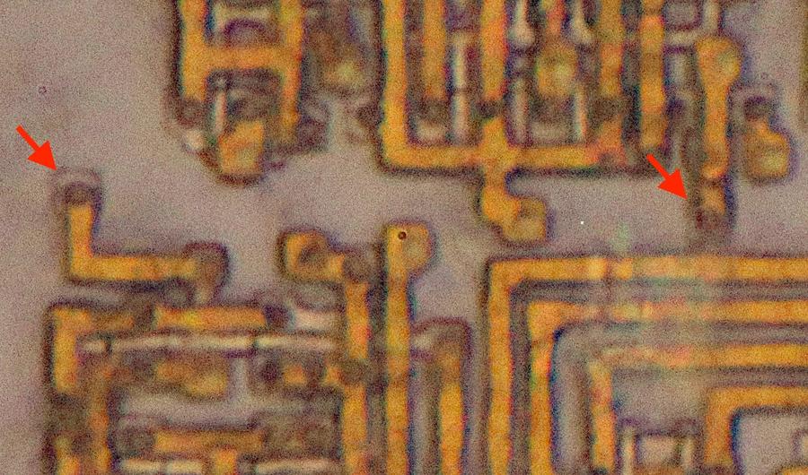
I was studying the silicon die of the Pentium processor and noticed some puzzling structures where signal lines were connected to the silico...

eBook: Pre-requisites for successful high-performance electronic system design.


There are many chip partitioning and placement tradeoffs when comparing top-tier smartphone processor designs.
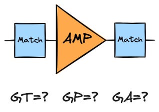
Transducer, Unilateral, Available and Power Gain; what they mean and how to calculate them.

Basic concepts required to understand classes of operation in power amplifiers.

Also known as the source follower, the common-drain amplifier is notable for its low output impedance. This article introduces the basic common-drain configuration and examines its large-signal characteristics.
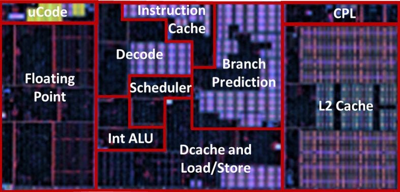
When I recently interviewed Mike Clark, he told me, “…you’ll see the actual foundational lift play out in the future on Zen 6, even though it was really Zen 5 that set the table for that.” And at that same Zen 5 architecture event, AMD’s Chief Technology Officer Mark Papermaster said, “Zen 5 is a ground-up redesign of the Zen architecture,” which has brought numerous and impactful changes to the design of the core.

Chip Creation Made Simple
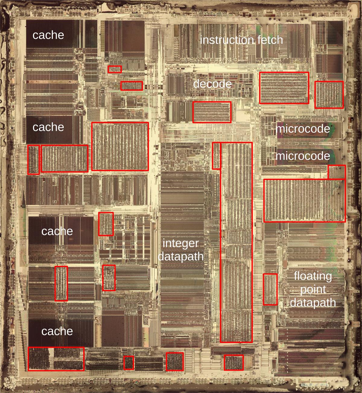
Intel released the powerful Pentium processor in 1993, a chip to "separate the really power-hungry folks from ordinary mortals." The origin...

This article explains how to successfully integrate logic gates into an LTspice simulation.

In this article, we use a SPICE model for 90 nm CMOS to plot key electrical relationships of an NMOS transistor.

SPICE models designed for specific CMOS process nodes can enhance simulations of integrated-circuit transistors. Learn where to find these models and how to use them.

In the realm of hardware design and verification, SystemVerilog stands as a titan among languages, beckoning engineers and developers with its robust capabilities. Originating from the fusion of Verilog with hardware verification languages, SystemVerilog’s evolution has revolutionized the world of electronic design automation (EDA). An introduction to SystemVerilog not only unfolds the story of its

A technical paper titled “Basilisk: Achieving Competitive Performance with Open EDA Tools on an Open-Source Linux-Capable RISC-V SoC” was published by researchers at ETH Zurich and University of Bologna. Abstract: “We introduce Basilisk, an optimized application-specific integrated circuit (ASIC) implementation and design flow building on the end-to-end open-source Iguana system-on-chip (SoC). We present enhancements to... » read more
DRAM research is difficult. Work that aims to be applicable to commodity devices should consider the sense amplifier internal layouts, transistor dimensions and circuit typologies used by real devices. These are all essential elements that must be considered while proposing new ideas. Unfortunately, they are not disclosed by DRAM vendors. As such, researchers are forced… Read
This paper aims to provide insights into the thermal, analog, and RF attributes, as well as a novel modeling methodology, for the FinFET at the industry standard 5nm CMOS technology node. Thermal characterization shows that for a 165K change in temperature, the Sub-threshold Slope (SS) and threshold voltage vary by 69 % and ~70 mV, respectively. At room temperature, a single gate contacted n-FinFET RF device exhibits a cutoff and maximum oscillation frequency of ~100 GHz and ~170 GHz, respectively. Analog and RF Figures of Merit (FoMs) for 5 nm technology at a device level and their temperature sensitivity are also reported. The industry standard BSIM-CMG model is modified to capture the impact of self-heating (SH) and parasitics. The SH model is based on measured data, and the modeling approach renders it independent of other model parameters. To the authors’ knowledge, an iteration free approach to develop a model-card for RF applications is explained for the very first time. Excellent agreement between the measured data and the model indicates that our methodology is accurate and can be used for faster PDK development.

In semiconductor design, “sign-off” during the tape-out (tapeout) of a chip refers to the formal approval process to ensure that the chip design is error-free, meets all specifications, and is ready for manufacturing at the foundry. It is essential because it minimizes the risk of costly errors, ensures compliance with foundry requirements, and validates that
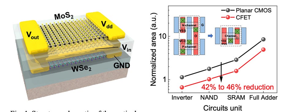
Planar to FinFET to Nanosheet to Complementary FET to 2D

Study tries to settle a bitter disagreement over Google’s chip design AI
While terms often are used interchangeably, they are very different technologies with different challenges.

RDL, an abbreviation for Redistribution Layer, that is, to make one or more layers of metal on the active chip side to redistribute the pins of the chip.
Historically Intel put all its cumulative chip knowledge to work advancing Moore's Law and applying those learnings to its future CPUs. Today, some of

Intel's multi-die interconnect bridge (EMIB) is an approach to in-package high-density interconnect of heterogeneous chips.

Powered by the promises of the CHIPS Act, Intel is investing more than $100 billion to increase domestic chip manufacturing capacity and capabilities.
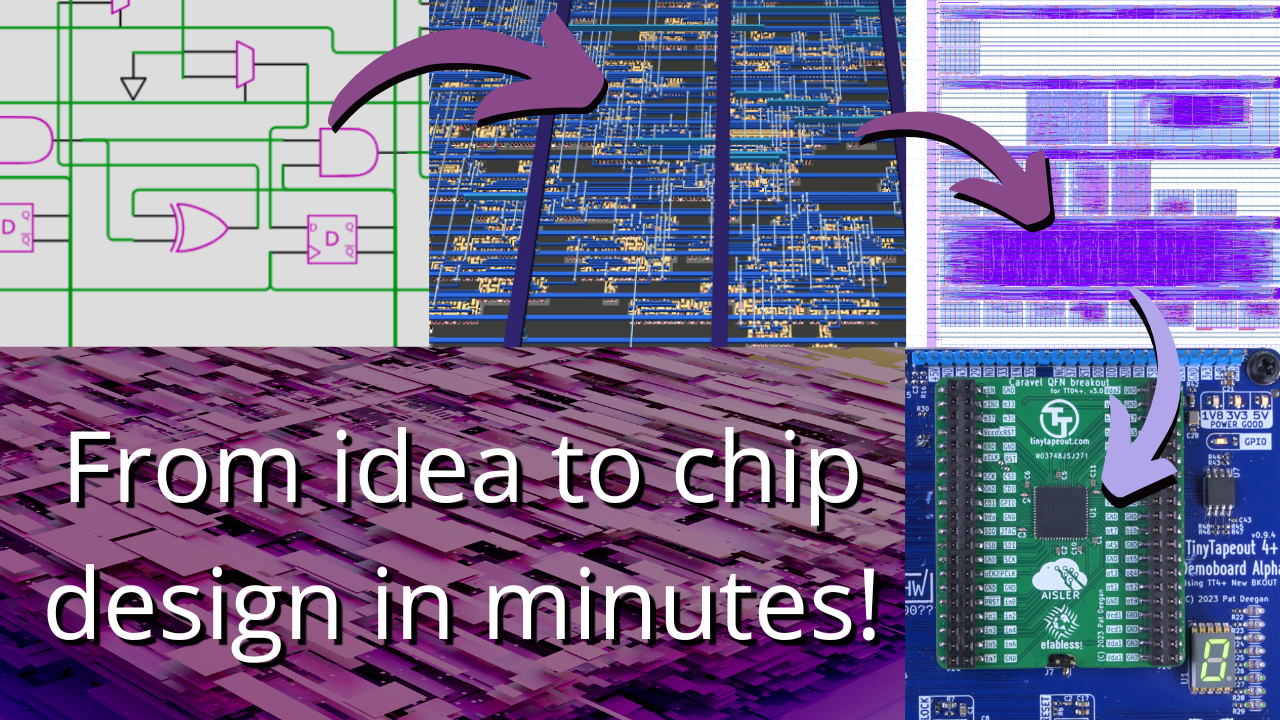
From idea to chip design in minutes! TT09 Closes in TT09 Closes in 44 DAYS 44 HOURS 44 MINS 44 SECS Tiles PCBs Tiny Tapeout is an educational project that makes it easier and cheaper than ever to get your designs manufactured on a real chip! Read the paper here. See what other people are making by taking a look at what was submitted on our previous shuttles.

A new technical paper titled “APOSTLE: Asynchronously Parallel Optimization for Sizing Analog Transistors Using DNN Learning” was published by researchers at UT Austin and Analog Devices. Abstract “Analog circuit sizing is a high-cost process in terms of the manual effort invested and the computation time spent. With rapidly developing technology and high market demand, bringing... » read more
Simulate electronic circuit using Python and the Ngspice / Xyce simulators - thejackal360/OpenSPICE

Achieving better signal integrity in a PCB design can be a challenge. Learn how PCB trace impedance variation plays a role, and how advanced tools can help smooth the way.

AI firm Synopsys has announced that its DSO.ai tool has successfully aided in the design of 100 chips, and it expects that upward trend to continue.
Book repository "Analysis and Design of Elementary MOS Amplifier Stages" - bmurmann/Book-on-MOS-stages

The following is a list of my articles on various topics. Besides technical articles, news pieces that might have useful technical information are also included. You can find my articles on FPGA...

Open Circuits: The Inner Beauty of Electronics is a visual feast for those who love electronics.

Learn about voltage waves and how they relate to an important basic concept of radio frequency (RF) circuit design: transmission lines.
The groundbreaking 8086 microprocessor was introduced by Intel in 1978 and led to the x86 architecture that still dominates desktop and se...

Interconnects—those sometimes nanometers-wide metal wires that link transistors into circuits on an IC—are in need of a major overhaul. And as chip fabs march toward the outer reaches of Moore’s Law, interconnects are also becoming the industry’s choke point.
Book repository "Analysis and Design of Elementary MOS Amplifier Stages" - bmurmann/Book-on-MOS-stages
A vast majority of modern digital integrated circuits are synchronous designs. They rely on storage elements called registers or flip-flops, all of which change their stored data in a lockstep manner with respect to a control signal called the clock. In many ways, the clock signal is like blood flowing through the veins of a

The high frequencies and data rates involved in 5G designs makes layout verification all the more important.

New technical paper titled “Bridging the Gap between Design and Simulation of Low-Voltage CMOS Circuits” from researchers at Federal University of Santa Catarina, Brazil. Abstract “This work proposes a truly compact MOSFET model that contains only four parameters to assist an integrated circuits (IC) designer in a design by hand. The four-parameter model (4PM) is... » read more
New technical paper titled “A Review on Transient Thermal Management of Electronic Devices” from researchers at Indian Institute of Technology Bombay. Abstract “Much effort in the area of electronics thermal management has focused on developing cooling solutions that cater to steady-state operation. However, electronic devices are increasingly being used in applications involving time-varying workloads. These... » read more

The researchers are considered a key to the company’s future. But they have had a hard time shaking infighting and controversy over a variety of issues.

When you’re baking a cake, it’s hard to know when the inside is in the state you want it to be. The same is true—with much higher stakes—for microelectronic chips: How can engineers confirm that what’s inside has truly met the intent of the designers? How can a semiconductor design company tell wh
An integrated cache and memory access time, cycle time, area, leakage, and dynamic power model - HewlettPackard/cacti

This article presents an LTspice circuit that can be used to explore the behavior of a phase-locked loop.
Magic VLSI: Resource Page
Silvaco provides standard cell library design and optimization services
I have written a lot of articles looking at leading…

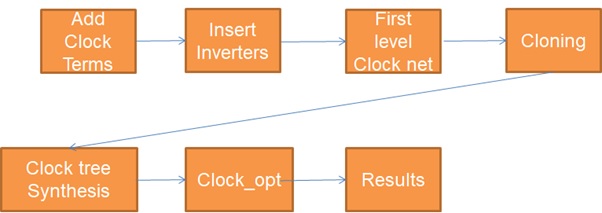
SoC clock tree overview, metrics that help qualify a clock tree and most commonly used clock tree distribution methodologies.
File formats used by EDA tools.

Some things will get better from a design perspective, while others will be worse.
New interconnects offer speed improvements, but tradeoffs include higher cost, complexity, and new manufacturing challenges.
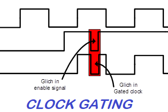
Clock Gating is defined as: “Clock gating is a technique/methodology to turn off the clock to certain parts of the digital design when not needed”. The Need for Clock Gating With most of the SoCs heavily constrained by power budgets, it is of utmost importance to reduce power consumption as much as possible

Leakage current can contribute to power dissipation, especially at lower threshold voltages. Learn about six types of leakage current that can be found in MOS transistors.
Gate-all-around FETs will replace finFETs, but the transition will be costly and difficult.

How can you calculate the number of dies per wafer? A free online tool, DPW equation and reference to two other DPW calculators. Trusted by Amkor and GF.
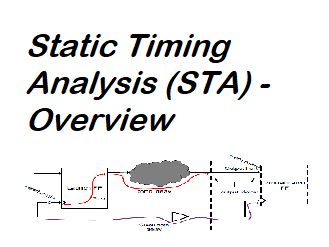
Static Timing Analysis? Read here the best overview to STA, including theory, real examples, ilustrations, tips and tricks.

In this article, we’ll discuss another group of thermal data, called thermal characterization parameters denoted by the Greek letter Psi (Ψ).

DIE YIELD CALCULATOR Use this online calculator to figure out die yield using Murphy’s model. You’ll need to know the die size, wafer diameter, and defect density. iSine is your complete resource for ASIC design – from concept to manufacturing and testing. We have expertise in system architecture, VHDL, Verilog, gate arrays, mixed signal, full...

Learn about an important thermal metric for designing the interface between an IC package and a heat sink.

Watch the thermal measurement, junction-to-case thermal resistance, in action as we use it to calculate the thermal considerations for a given system.

Engineers must keep pace with advanced IC packaging technology as it evolves rapidly, starting with understanding the basic terms.

Assessing the thermal performance of an IC package becomes easier if you understand this common, but often misapplied, parameter known as theta JA.

In this article, we will learn how to find the optimal size of a transistor/logic gate present in a larger circuit to provide the desired performance using the linear delay model.
When they were first commercialized at the 22 nm node, finFETs represented a revolutionary change to the way we build transistors, the tiny switches in the “brains” of a chip. As compared to...

In this article, we'll discuss the Elmore delay model, which provides a simplistic delay analysis that avoids time-consuming numerical integration/differential equations of an RC network.
The semiconductor industry growth is increasing exponentially with high speed…
Looking at a typical SoC design today it's likely to…

Single-clock design is not always as easy as it seems.
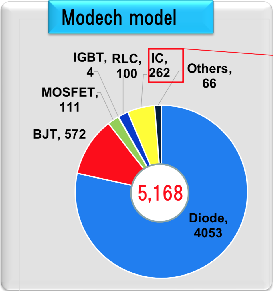
SPICE (Simulation Program with Integrated Circuit Emphasis) is an open-source analog electronic circuit simulator. | SPICE is undoubtedly one of the most popular modeling libraries available, and Japanese e-commerce company MoDeCH is seeking to make the power of SPICE available to everyone.

Accurately determine parasitic effects with the proper set up of two different methods.

Process Corner Explosion, At 7nm and below, modeling what will actually show up in silicon is a lot more complicated.

Post date: Sep 19, 2014 10:01:08 PM

Design, operation and characteristics of the most linear amplifier class of all.

Haptic feedback systems using piezo-based actuators are important for a variety of applications, especially automotive. Learn the challenges and the solutions to be considered for this technology.

Fab Cost, WFE Implications, Backside Power Details