sram


A new technical paper titled “Prefill vs. Decode Bottlenecks: SRAM-Frequency Tradeoffs and the Memory-Bandwidth Ceiling” was published by researchers at Uppsala University. Abstract “Energy consumption dictates the cost and environmental impact of deploying Large Language Models. This paper investigates the impact of on-chip SRAM size and operating frequency on the energy efficiency and performance of... » read more

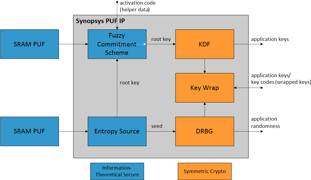
Discover SRAM PUF’s security benefits and how Synopsys combines it with OTP memory for advanced, secure key storage in embedded systems.
Compute-in-SRAM architectures offer a promising approach to achieving higher performance and energy efficiency across a range of data-intensive applications. However, prior evaluations have largely relied on simulators or small prototypes, limiting the understanding of their real-world potential. In this work, we present a comprehensive performance and energy characterization of a commercial compute-in-SRAM device, the GSI APU, under realistic workloads. We compare the GSI APU against established architectures, including CPUs and GPUs, to quantify its energy efficiency and performance potential. We introduce an analytical framework for general-purpose compute-in-SRAM devices that reveals fundamental optimization principles by modeling performance trade-offs, thereby guiding program optimizations. Exploiting the fine-grained parallelism of tightly integrated memory-compute architectures requires careful data management. We address this by proposing three optimizations: communication-aware reduction mapping, coalesced DMA, and broadcast-friendly data layouts. When applied to retrieval-augmented generation (RAG) over large corpora (10GB--200GB), these optimizations enable our compute-in-SRAM system to accelerate retrieval by 4.8$\times$--6.6$\times$ over an optimized CPU baseline, improving end-to-end RAG latency by 1.1$\times$--1.8$\times$. The shared off-chip memory bandwidth is modeled using a simulated HBM, while all other components are measured on the real compute-in-SRAM device. Critically, this system matches the performance of an NVIDIA A6000 GPU for RAG while being significantly more energy-efficient (54.4$\times$-117.9$\times$ reduction). These findings validate the viability of compute-in-SRAM for complex, real-world applications and provide guidance for advancing the technology.
Fully integrated dToF modules and iToF VCSEL illuminators for short range applications. Laser sources for long range LIDAR systems.

The idea isn't novel, but presents major challenges. Tensordyne thinks it has solved them, and promises massive speed and efficiency gains as a result.

A new technical paper titled “Energy-Accuracy Trade-Offs in Massive MIMO Signal Detection Using SRAM-Based In-Memory Computing” was published by researchers at the University of Illinois at Urbana–Champaign. Abstract “This paper investigates the use of SRAM-based in-memory computing (IMC) architectures for designing energy efficient and accurate signal detectors for massive multi-input multi-output (MIMO) systems. SRAM-based IMCs... » read more
Traditional von Neumann architectures suffer from fundamental bottlenecks due to continuous data movement between memory and processing units, a challenge that worsens with technology scaling as electrical interconnect delays become more significant. These limitations impede the performance and energy efficiency required for modern data-intensive applications. In contrast, photonic in-memory computing presents a promising alternative by harnessing the advantages of light, enabling ultra-fast data propagation without length-dependent impedance, thereby significantly reducing computational latency and energy consumption. This work proposes a novel differential photonic static random access memory (pSRAM) bitcell that facilitates electro-optic data storage while enabling ultra-fast in-memory Boolean XOR computation. By employing cross-coupled microring resonators and differential photodiodes, the XOR-augmented pSRAM (X-pSRAM) bitcell achieves at least 10 GHz read, write, and compute operations entirely in the optical domain. Additionally, wavelength-division multiplexing (WDM) enables n-bit XOR computation in a single-shot operation, supporting massively parallel processing and enhanced computational efficiency. Validated on GlobalFoundries' 45SPCLO node, the X-pSRAM consumed 13.2 fJ energy per bit for XOR computation, representing a significant advancement toward next-generation optical computing with applications in cryptography, hyperdimensional computing, and neural networks.

Table of Contents Motivation Optimization goal of GPUs Key concepts of GPUs - software and...
Number of designs that are late increases. Rapidly rising complexity is the leading cause, but tools, training, and workflows need to improve.
The move to nanosheet transistors is a boon for SRAM
After persistent rumors refused to recede, AMD steps in with a clear explanation why dual-CCD V-Cache doesn't exist.

Compute costs scale with the square of the input size. That’s not great.

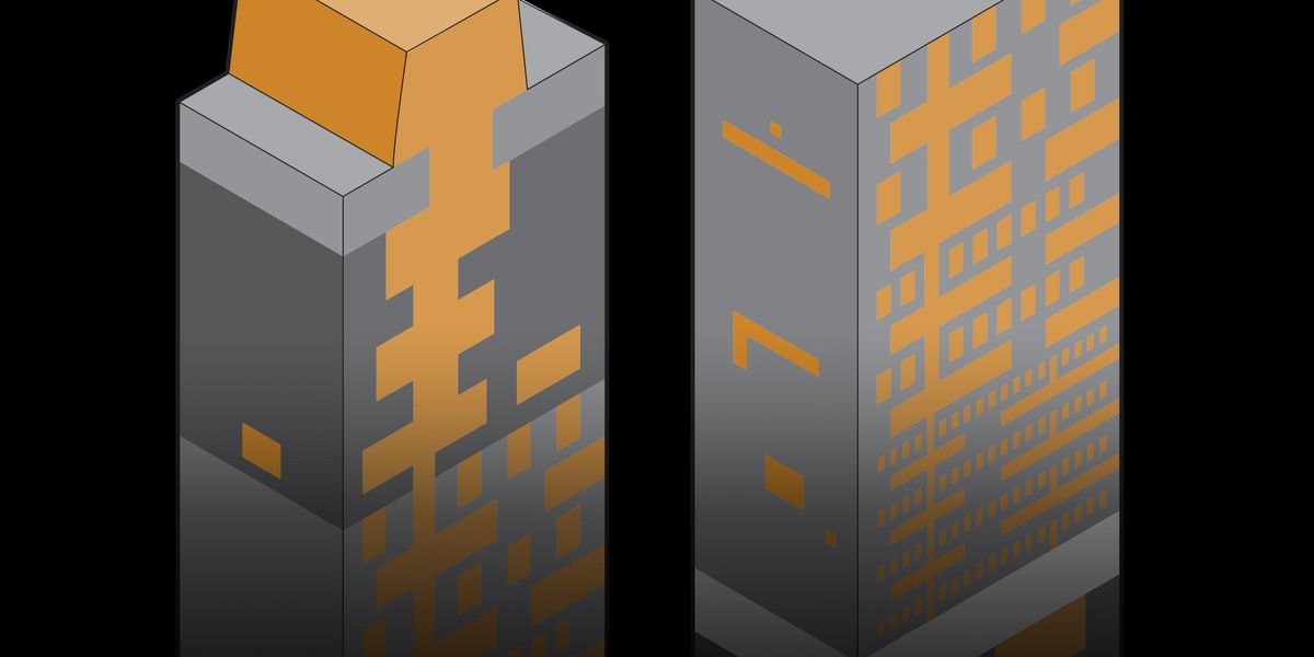
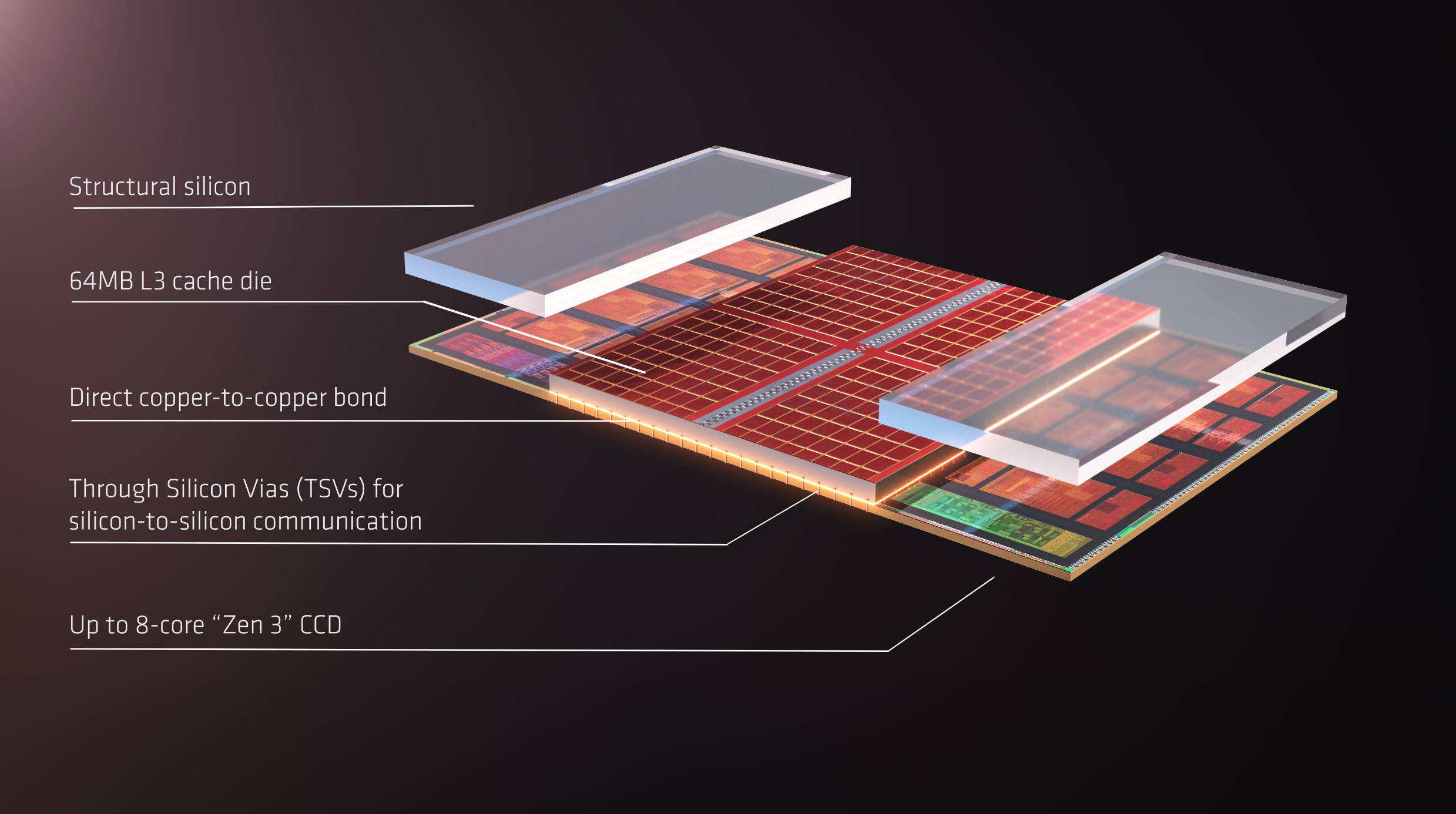
The CCD stack with 3D V-Cache on the AMD Ryzen 7 9800X3D is only 40-45µm in total, but the rest of the layers add up to a whopping 750µm.

Large Language Models (LLMs) have become a cornerstone of artificial intelligence, driving advancements in natural language processing and decision-making tasks. However, their extensive power demands, resulting from high computational overhead and frequent external memory access, significantly hinder their scalability and deployment, especially in energy-constrained environments such as edge devices. This escalates the cost of operation while also limiting accessibility to these LLMs, which therefore calls for energy-efficient approaches designed to handle billion-parameter models. Current approaches to reduce the computational and memory needs of LLMs are based either on general-purpose processors or on GPUs, with a combination of weight quantization and

And Intel shows how far these devices could go

It hasn’t achieved commercial success, but there is still plenty of development happening; analog IMC is getting a second chance.
Notes from the Latent Space paper club. Follow along or start your own! - eugeneyan/llm-paper-notes


As awareness of environmental, social, and governance (ESG) issues grows, companies are adopting strategies for sustainable operations.

There are many chip partitioning and placement tradeoffs when comparing top-tier smartphone processor designs.

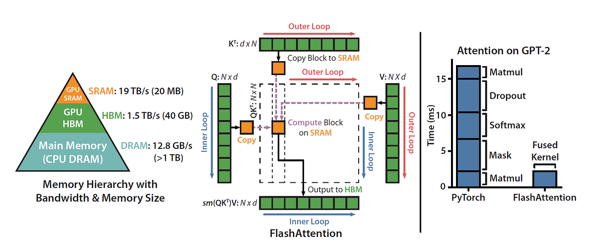
Attention, as a core layer of the ubiquitous Transformer architecture, is a bottleneck for large language models and long-context applications. FlashAttention (and FlashAttention-2) pioneered an approach to speed up attention on GPUs by minimizing memory reads/writes, and is now used by most libraries to accelerate Transformer training and inference. This has contributed to a massive increase in LLM context length in the last two years, from 2-4K (GPT-3, OPT) to 128K (GPT-4), or even 1M (Llama 3). However, despite its success, FlashAttention has yet to take advantage of new capabilities in modern hardware, with FlashAttention-2 achieving only 35% utilization of theoretical max FLOPs on the H100 GPU. In this blogpost, we describe three main techniques to speed up attention on Hopper GPUs: exploiting asynchrony of the Tensor Cores and TMA to (1) overlap overall computation and data movement via warp-specialization and (2) interleave block-wise matmul and softmax operations, and (3) incoherent processing that leverages hardware support for FP8 low-precision.
The impact of quantum algorithms on different cryptographic techniques and what can be done about it.

Imec’s plan to use superconductors to shrink computers
Volatile memory threat increases as chips are disaggregated into chiplets, making it easier to isolate memory and slow data degradation.

We present a predictive process design kit (PDK) for the 5 nm technology node, the ASAP5 PDK. ASAP5 is not related to a particular foundry and the ass…
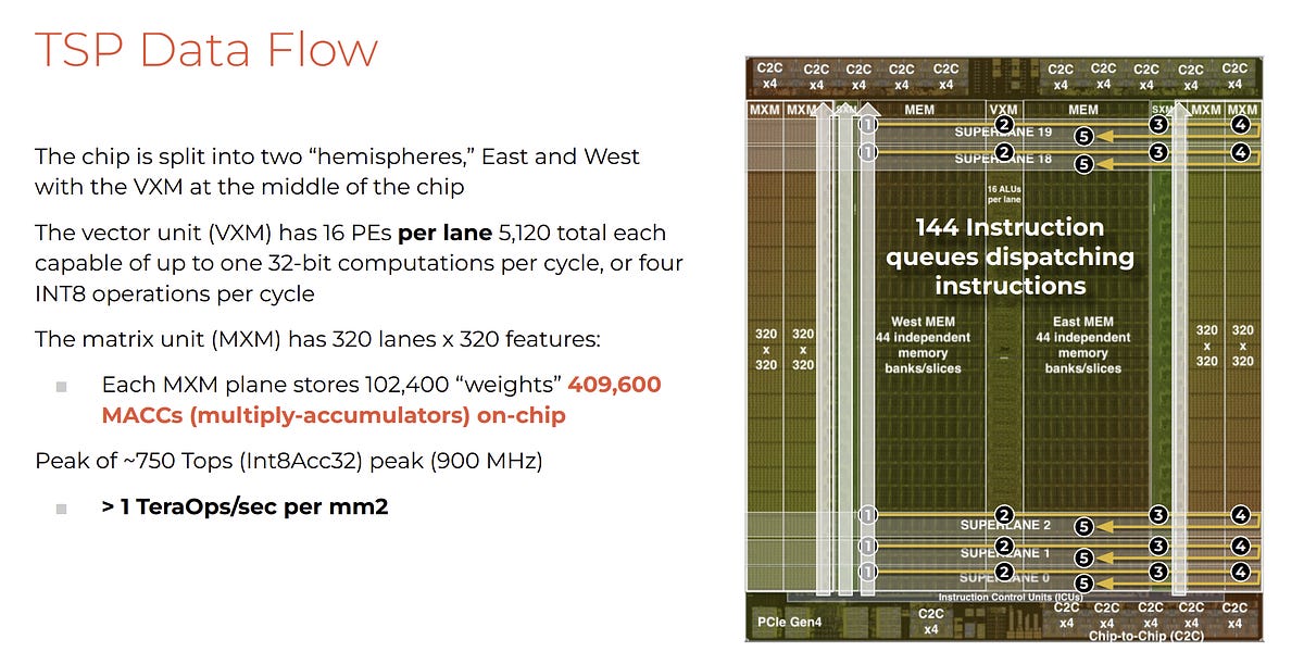
Startup Groq has developed an machine learning processor that it claims blows GPUs away in large language model workloads – 10x faster than an Nvidia GPU at 10 percent of the cost, and needing a tenth of the electricity. Update: Groq model compilation time and time from access to getting it up and running clarified. […]
Faster than Nvidia? Dissecting the economics
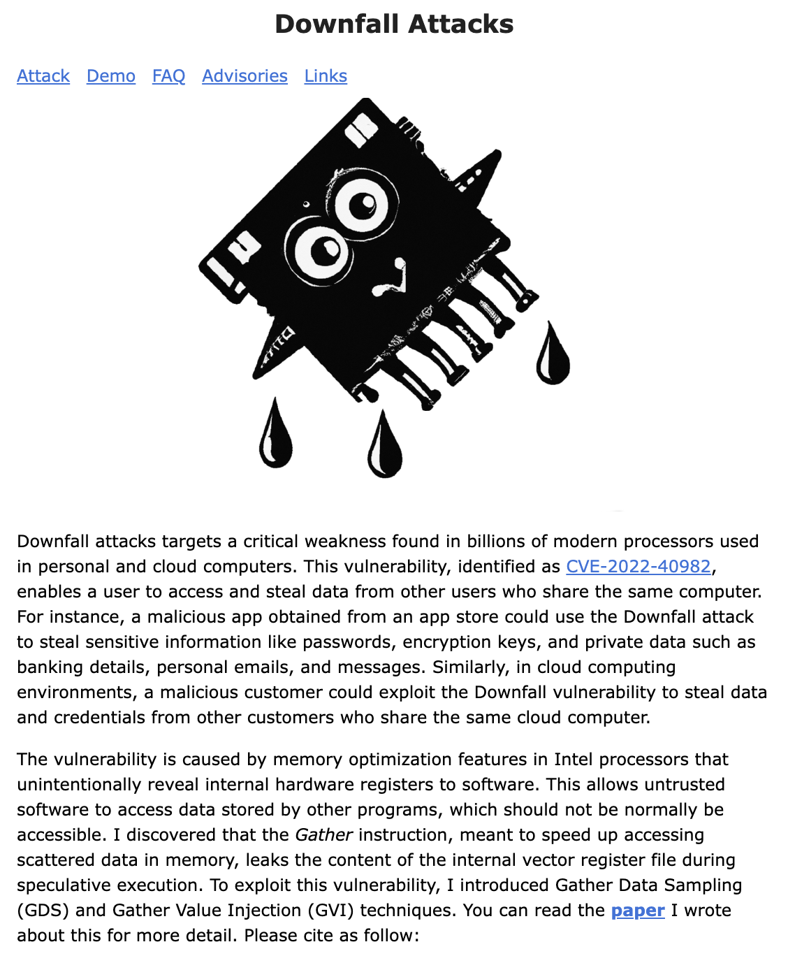
Downfall attacks targets a critical weakness found in billions of modern processors used in personal and cloud computers.

Atom-thin layers of oxygen in a chip’s silicon can make devices speedier and more reliable
Step by step explanation of how one of the most important MLSys breakthroughs work — in gory detail.

A technical paper titled “Benchmarking and modeling of analog and digital SRAM in-memory computing architectures” was published by researchers at KU Leuven. Abstract: “In-memory-computing is emerging as an efficient hardware paradigm for deep neural network accelerators at the edge, enabling to break the memory wall and exploit massive computational parallelism. Two design models have surged:... » read more

tldr; techniques to speed up training and inference of LLMs to use large context window up to 100K input tokens during training and…
Editor’s Note (6/14/2023): We have a new article that reevaluates the cache latency of Navi 31, so please refer to that article for some new latency data.
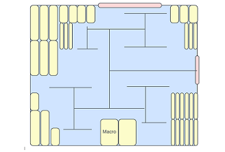
Floorplanning plays a crucial role in the physical design of an SoC and lays the foundation for an efficient and high-performance ASIC layout. In this article, we will discuss ten essential floorplanning commandments that physical design engineers can follow to ensure a correct-by-construction design. Design Partitioning Design Partitioning refers to dividing a large

New memory technologies have emerged to push the boundaries of conventional computer storage.
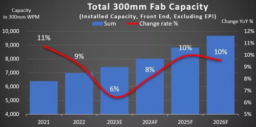
After dipping this year, the growth of 300mm semiconductor manufacturing capacity is set to gain momentum.
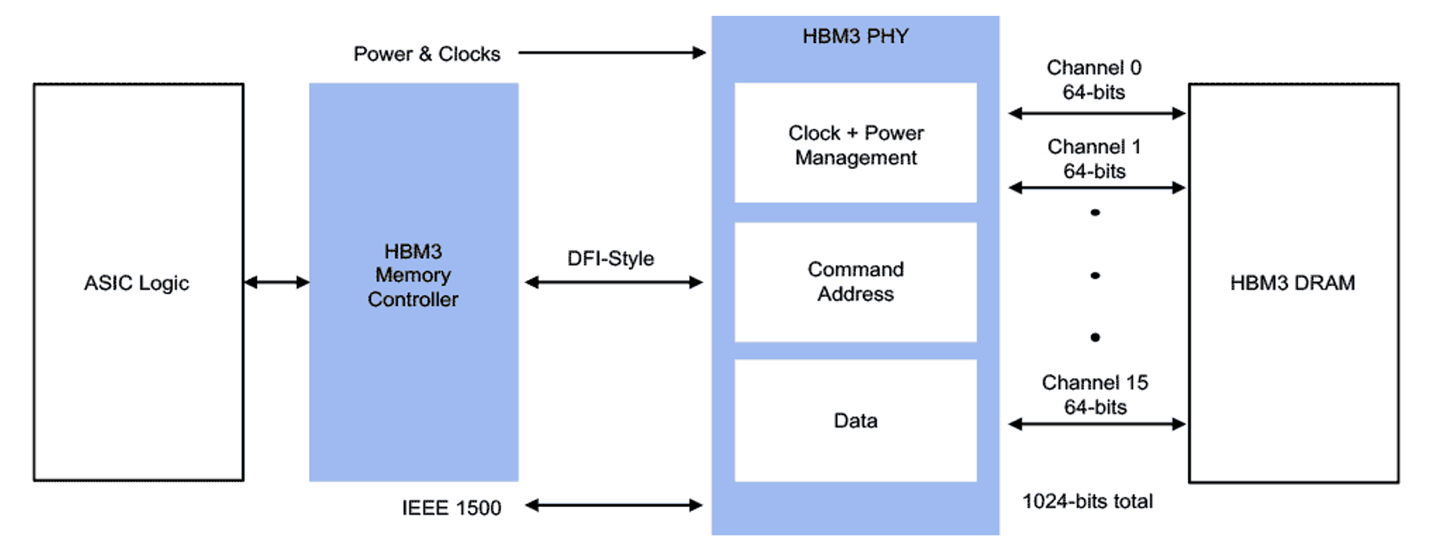
Sponsored Feature: Training an AI model takes an enormous amount of compute capacity coupled with high bandwidth memory. Because the model training can be
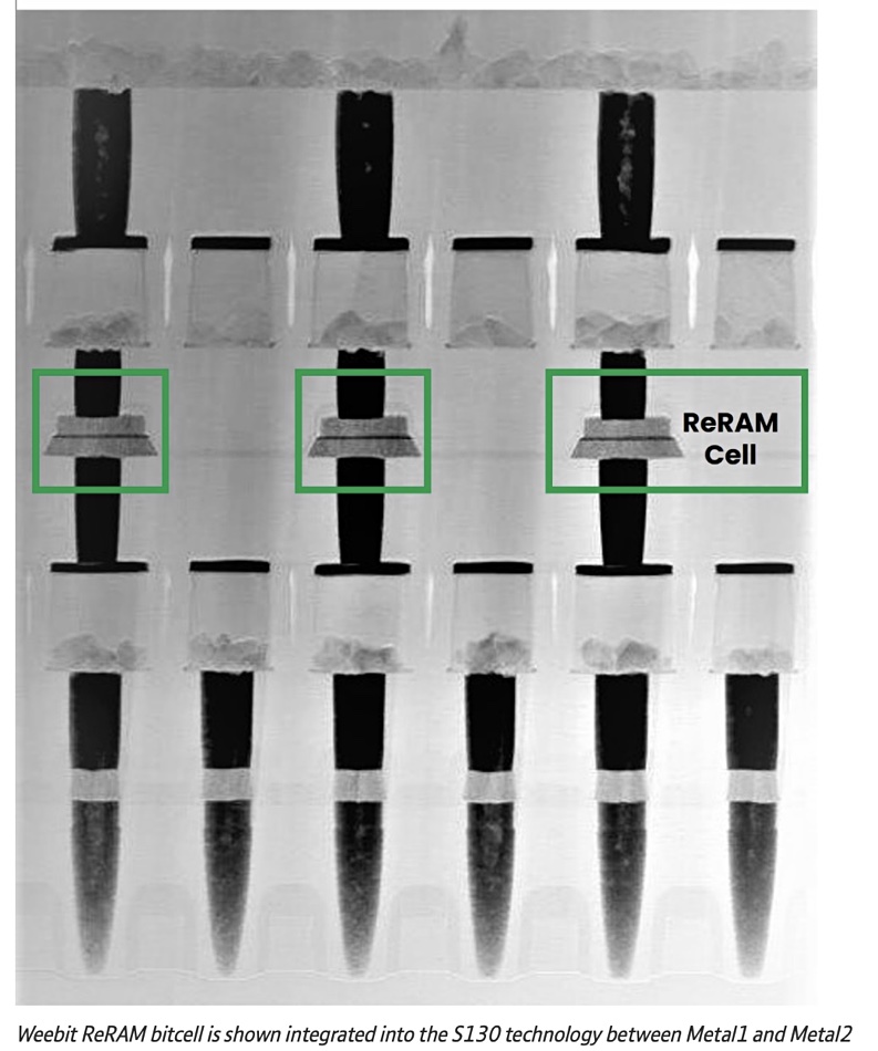
ReRAM startup Intrinsic Semiconductor Technologies has raised $9.73 million to expand its engineering team and bring its product to market.
Security IP cores are blocks that provide security features for integrated circuits (ICs) and systems-on-chips (SoCs). It includes encryption, decryption, authentication, and key management functions that protect against unauthorized access or hacking. The IP core can be integrated into a larger IC design to provide enhanced security for applications such as IoT devices, payment systems,
Industry sources say TSMC is considering lowering 3nm prices to stimulate interest from chip designers
List of awesome open source hardware tools, generators, and reusable designs - aolofsson/awesome-opensource-hardware

A technical paper titled “Beware of Discarding Used SRAMs: Information is Stored Permanently” was published by researchers at Auburn University. The paper won “Best Paper Award” at the IEEE International Conference on Physical Assurance and Inspection of Electronics (PAINE) Oct. 25-27 in Huntsville. Abstract: “Data recovery has long been a focus of the electronics industry... » read more

The world's largest chip scales to new heights.
Changes are steady in the memory hierarchy, but how and where that memory is accessed is having a big impact.
A vast majority of modern digital integrated circuits are synchronous designs. They rely on storage elements called registers or flip-flops, all of which change their stored data in a lockstep manner with respect to a control signal called the clock. In many ways, the clock signal is like blood flowing through the veins of a
Increased transistor density and utilization are creating memory performance issues.

Let's learn more about the world's most important manufactured product. Meaningful insight, timely analysis, and an occasional investment idea.
There are two types of packaging that represent the future of computing, and both will have validity in certain domains: Wafer scale integration and

EE Times Compares SRAM vs. DRAM, Common Issues With Each Type Of Memory, And Takes A Look At The Future For Computer Memory.
This blog post is in response to a recent topic on the Parallella forum regarding Adapteva’s chip cost efficiency (GFLOPS/$): [forum discussion thread]. I had to be a little vague on some poi…

Explore Synopsys Blog for the latest insights and trends in EDA, IP, and Systems Design. Stay updated with expert articles and industry news.
I have written a lot of articles looking at leading…
Currently there are more than 100 companies all over the world building ASIC’s (Application specific integrated circuit) or SOC’s (System…

Getting data in and out of memory faster is adding some unexpected challenges.

Experts at the Table: Which type of DRAM is best for different applications, and why performance and power can vary so much.

Evaluate inference accelerators to find the best throughput for the money.
Buried interconnects will help save Moore's Law

Some things will get better from a design perspective, while others will be worse.
New interconnects offer speed improvements, but tradeoffs include higher cost, complexity, and new manufacturing challenges.
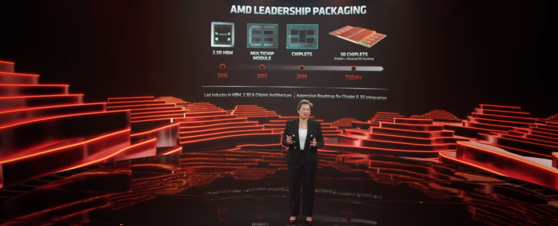
AMD recently unveiled 3D V-Cache, their first 3D-stacked technology-based product. Leapfrogging contemporary 3D bonding technologies, AMD jumped directly into advanced packaging with direct bonding and an order of magnitude higher wire density.

Pushing AI to the edge requires new architectures, tools, and approaches.

SRAM cell architecture introduction: design and process challenges assessment.
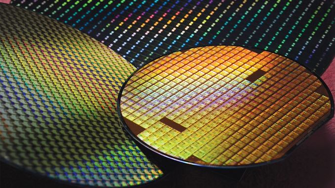
This is a list of semiconductor fabrication plants. A semiconductor fabrication plant is where integrated circuits (ICs), also known as microchips, are manufactured. They are either operated by Integrated Device Manufacturers (IDMs) that design and manufacture ICs in-house and may also manufacture designs from design-only (fabless firms), or by pure play foundries that manufacture designs from fabless companies and do not design their own ICs. Some pure play foundries like TSMC offer IC design services, and others, like Samsung, design and manufacture ICs for customers, while also designing, manufacturing and selling their own ICs.
But so are better approaches to deal with thorny counterfeiting issues.
Looking at a typical SoC design today it's likely to…
What is the hardest job at Intel, excepting whoever is in charge of the development of chip etching processes and the foundries that implement it? We
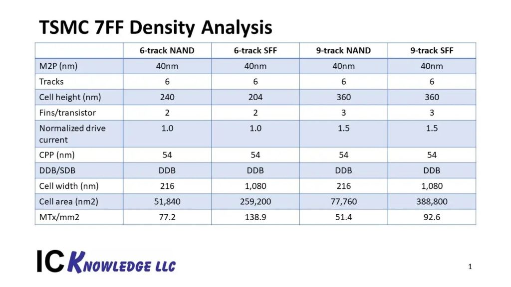
TSMC details its 5-nanometer node for mobile and HPC applications. The process features the industry's highest density transistors with a high-mobility channel and highest-density SRAM cells.

"...Google's people analytics experts had been studying how to onboard new hires effectively. They came back with a list of tips. Here’s the one that jumped…
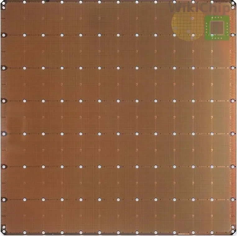
A look at Cerebras Wafer-Scale Engine (WSE), a chip the size of a wafer, packing over 400K tiny AI cores using 1.2 trillion transistors on a half square foot of silicon.

Why MRAM is so attractive.

TOPS isn't all you need to know about an inference chip.

Researchers at imec explore strategy that could make memory more efficient and pack in more transistors

Areanna claims that a custom SRAM delivers 100 TOPS/W on deep learning, but it’s early days for the startup.
How the wrong benchmark can lead to incorrect conclusions.

The previous post in this series (excerpted from the Objective Analysis and Coughlin Associates Emerging Memory report) explained why emerging memories are necessary. Oddly enough, this series will explain bit selectors before defining all of the emerging memory technologies themselves. The reason why is that the bit selector determines how small a bit cell can

Processing In Memory Growing volume of data and limited improvements in performance create new opportunities for approaches that never got off the ground.

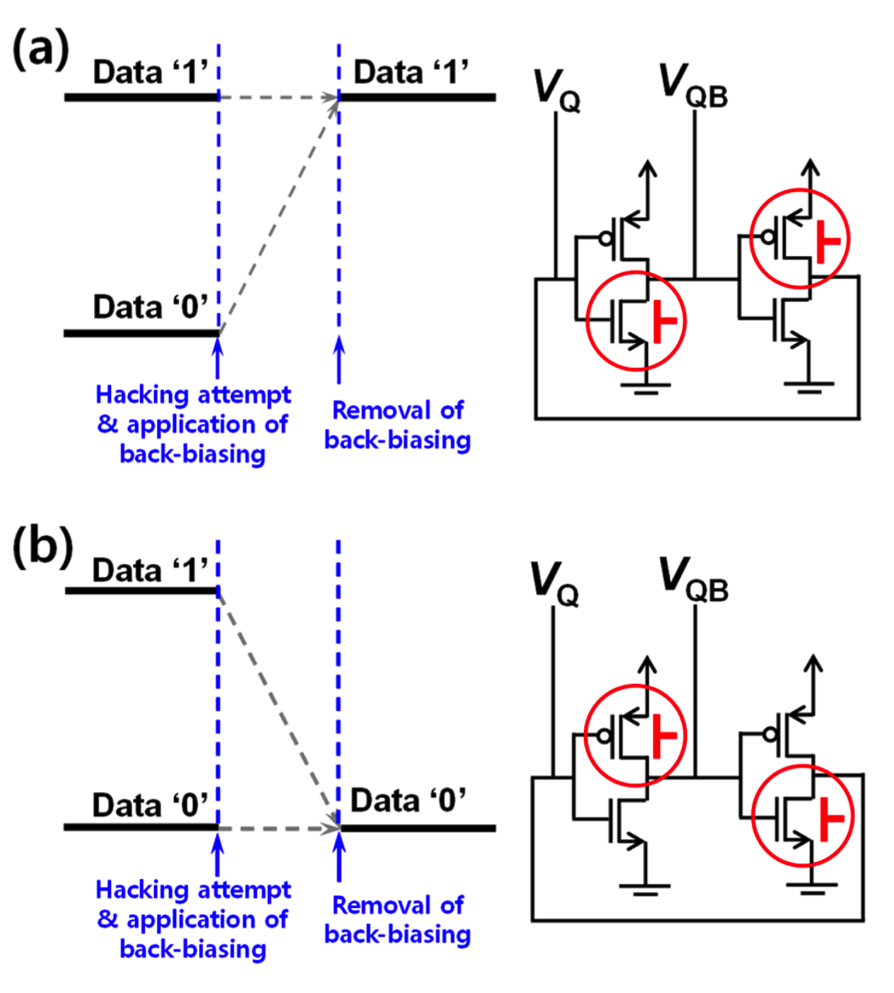
Imperfect Silicon, Near-Perfect Security Physically unclonable functions (PUF) seem tailor-made for IoT security.

Katherine Bourzac / IEEE Spectrum: The Northwest-AI-Hub, which is researching hybrid gain cell memory that combines DRAM's density with SRAM's speed, gets a $16.3M CHIPS Act grant via the US DOD

Researchers developing dense, speedy hybrid gain cell memory recently got a boost from CHIPS Act funding

Fab Cost, WFE Implications, Backside Power Details