DRAM-SRAM-NVM

Kioxia and Sandisk haVE started delivering samples of its tenth generation 3D NAND BiCS chips w ...
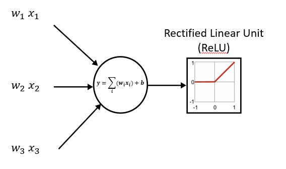
Learning from a classic AI accelerator - Eyeriss

Intel announced this week that it’s working with SoftBank subsidiary SAIMEMORY to commercialize Z-Angle Memory (ZAM), an advanced type of DRAM that stacks memory modules vertically. While ZAM chips aren’t expected to become available for at least three years, they could eventually replace the high-bandwidth memory (HBM) that is in such high demand today thanks […]
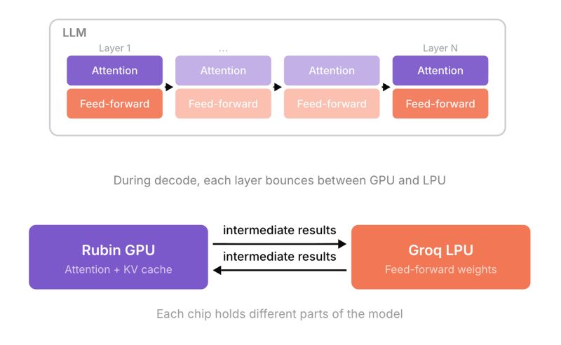
why did NVIDIA cancel the Rubin CPX and replace it with a Groq LPU? LLM inference has two phases. prefill processes the whole prompt at once and is compute-bound. decode generates one token at a time and is memory-bound, reading the full model weights and KV cache for every token. since 2024 the standard approach has been splitting these onto separate GPU pools so prefill and decode stop interfering with each other. NVIDIA's first hardware answer was the Rubin CPX, announced September 2025. a dedicated prefill chip with 128 GB of GDDR7 memory, over 50% cheaper per GB than HBM, under 800W, more chips per rack. prefill is compute-bound, so save the expensive HBM for decode. the savings were real, but regular Rubin GPUs also handle prefill well enough. six months later at GTC 2026, NVIDIA shelved the CPX and partnered with Groq on a completely different split. Groq's split happens inside each layer. every transformer layer has an attention block that reads the KV cache and a feed-forward block that reads only its own weights. the KV cache is tens of gigabytes and is stored in HBM on the GPU. the feed-forward weights are smaller and read the same way every token. that second property is the reason SRAM works here. the Groq LP30 has 500 MB of on-chip SRAM at 150 TB/s, about 20x the memory bandwidth of a B200's HBM3e. run feed-forward on the LP30, keep attention on the GPU, and pass intermediate results between them at every layer. NVIDIA calls it Attention-FFN Disaggregation. the LPX rack packs 256 LP30 chips for 128 GB of SRAM and 40 PB/s aggregate bandwidth, with 640 TB/s of chip-to-chip interconnect for the per-layer transfer. NVIDIA claims 35x more inference throughput per megawatt than GB200 NVL72. so the short answer: the CPX saved cost on prefill, where regular GPUs were already fine. AFD delivers 20x bandwidth on decode by splitting inside the layer, where the real bottleneck sits. different axis, bigger win. wrote up the full details on the blog with diagrams for each approach, plus the AWS + Cerebras split where Trainium handles prefill and a wafer-scale CS-3.

Disaggregated inference started as a software technique for splitting prefill and decode onto separate GPU pools. NVIDIA, Groq, Cerebras, and AWS are now taking it further with chips purpose-built for each phase.

HBM, GDDR, and SRAM compared: how memory hierarchy, bandwidth, and capacity determine AI accelerator performance, cost, and which workloads each chip can serve.

Samsung has reportedly produced the world's first standalone DRAM module that uses a process tech below 10nm.

DRAM Market Shift: From Mobile to Infrastructure (2023–2030) The latest DRAM demand outlook highlights a clear structural transition: memory demand is moving from mobile-driven to infrastructure-driven growth. 1. Infrastructure Becomes Dominant Servers & Workstations grow from 34% (2023) to 53% (2030). Including HBM, infrastructure reaches: 38% → 61% of total DRAM demand This shift is driven by: AI training & inference Hyperscale cloud expansion GPU/accelerated computing architectures 👉 DRAM is increasingly a performance bottleneck, not just capacity. 2. Smartphones Lose Relative Share Smartphones decline from 34% → 17%. This reflects: Market maturity Efficiency gains Faster growth elsewhere The industry is shifting from: Volume growth → Bandwidth & performance growth 3. HBM: Small Share, Strategic Impact HBM grows from 4% to ~8–10%, but its importance is disproportionate. Critical for AI scaling Highest value-per-bit segment Supply remains constrained 👉 This is where margin pools are moving. 4. Application & Product Trends Automotive 1% → 8% growth Transition: LPDDR4X → LPDDR5X → LPDDR6 Driven by ADAS and centralized compute PCs Slight share decline, but: More LPDDR adoption AI PC architectures emerging Consumer Electronics Gradual decline (15% → 6%) Limited performance-driven scaling 5. Capex & Industry Dynamics Investment focus is shifting toward: Advanced DRAM nodes (1β, 1γ) HBM capacity Advanced packaging (e.g., 3D stacking) At the same time: Supply discipline is tightening HBM remains structurally constrained 6. Strategic Takeaway This is not a typical cycle. It is a structural transformation of the DRAM industry, where: Infrastructure dominates demand HBM drives value creation Memory becomes central to compute performance Key question: Will HBM become the primary profit engine of the industry? #Semiconductors #DRAM #Memory #AI #ArtificialIntelligence #Cloud #CloudComputing #DataCenters #HBM #HighBandwidthMemory #Automotive #ADAS #EdgeComputing #AIInfrastructure #DDR5 #LPDDR5 #LPDDR6 #TechTrends #DigitalTransformation #Samsung #SamsungElectronics #SKHynix #Micron #Nanya #Winbond #PSMC #CXMT #ISSI #IntegratedSiliconSolution #IntelligentMemory #Longsys #BiWin #Kingston #ADATA #AdataTechnology #Apacer #TeamGroup #GSkill #Transcend

🚨 DDR4 / LPDDR4: The Beginning of the End — or a Strategic Reset? The memory industry is approaching a pivotal inflection point—and the signals are becoming impossible to ignore. Recent developments from Samsung indicate that legacy nodes such as LPDDR4 (and increasingly DDR4) are entering structured end-of-life (EOL) management. The most probable scenario? 📅 A major transition window between late 2026 and early 2027 But this is not simply a sunset story—it’s a strategic realignment of the entire DRAM ecosystem. A clear supplier bifurcation is emerging: 🟥 Tier-1 leaders: Accelerating the exit Samsung Semiconductor is leading the shift, reallocating capacity toward LPDDR5/LPDDR5X, DDR5, and AI-driven memory (HBM) SK hynix is expected to follow closely, driven by the same margin and technology imperatives The logic is straightforward: 👉 Legacy = volume but low margin 👉 Advanced nodes = lower volume, significantly higher profitability 🟧 Micron: The “delayed exit” strategy Micron Technology is likely to extend DDR4/LPDDR4 support longer Why? Automotive & industrial commitments Long qualification cycles Result: a phased, slower disengagement, not an abrupt exit 🟩 The structural gap fillers As Tier-1 players pivot, demand doesn’t disappear—it fragments This creates a persistent supply gap in mature nodes Key players stepping in: Nanya Technology → Optimizing DDR4 capacity & cost structures Winbond → Expanding specialty DRAM for industrial markets Intelligent Memory → Lifecycle-focused solutions for embedded/industrial applications 👉 Expect targeted capacity expansion, longer product lifecycles, and niche specialization What’s really happening? This is not just a node transition. It is a full ecosystem segmentation: • Leading-edge players → LPDDR5X, DDR5, HBM, AI • Mature-node specialists → DDR4 / LPDDR4 lifecycle continuity • OEMs → Forced to rethink sourcing strategies Demand for DDR4/LPDDR4 is NOT going away, it is simply becoming structurally redistributed My perspective: We are witnessing a classic industry evolution: ➡️ Innovation leaders move up the value chain ➡️ Mature technologies don’t die—they get re-homed The real disruption is not technological—it is supply chain restructuring The key question: Who will dominate the “long tail” of memory demand once Tier-1 suppliers fully exit? Because that’s where the next strategic battleground is forming. Contact for longevity support: Nick Florous, Ph.D. MEMPHIS Electronic #DDR4 #LPDDR4 #DDR5 #LPDDR5X #Semiconductors #MemoryIndustry #SupplyChain #AutomotiveTech #IndustrialIoT #AI #TechStrategy #EOL

Rambus has announced its LPDDR5X SOCAMM2 memory chipset, a vital component to enable the next-gen compact memory for AI datacenters.

A new embedded memory architecture with a three-transistor cell.

Explore the four key modern memory types: ROM, DRAM, SRAM, and flash, their unique roles, and trade-offs in speed, cost, and storage.

A new technical paper titled “Functionally-Complete Boolean Logic in Real DRAM Chips: Experimental Characterization and Analysis” was published by researchers at ETH Zurich. Abstract: “Processing-using-DRAM (PuD) is an emerging paradigm that leverages the analog operational properties of DRAM circuitry to enable massively parallel in-DRAM computation. PuD has the potential to significantly reduce or eliminate costly... » read more
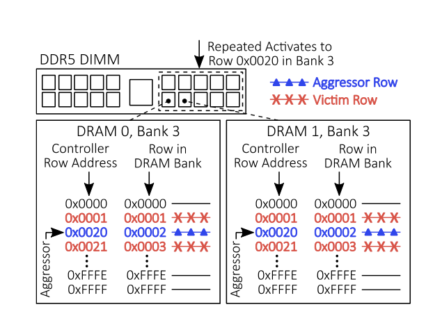
What it is, and why this has become such a significant security issue.
Need a New Year's resolution? How about stop paying for memory you don't need