Groq Inference Tokenomics: Speed, But At What Cost?
Faster than Nvidia? Dissecting the economics
Faster than Nvidia? Dissecting the economics
Embracing emerging approaches is essential for crafting packages that address the evolving demands of sustainability, technology, and consumer preferences.
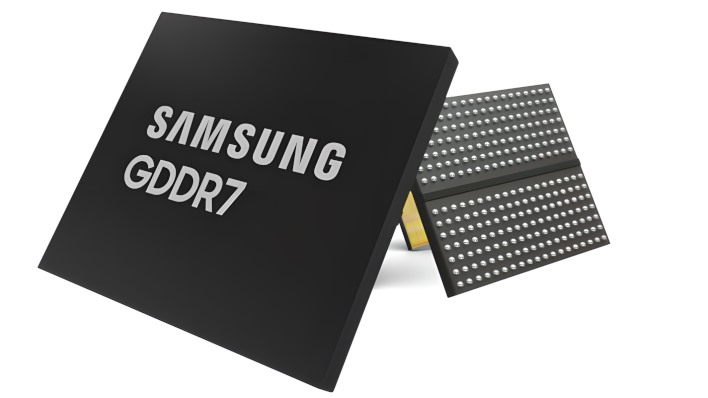
A conference schedule has revealed that Samsung's next-gen graphics memory is bonkers fast.
China's Countermove: How Beijing is Dodging New Semiconductor Restrictions
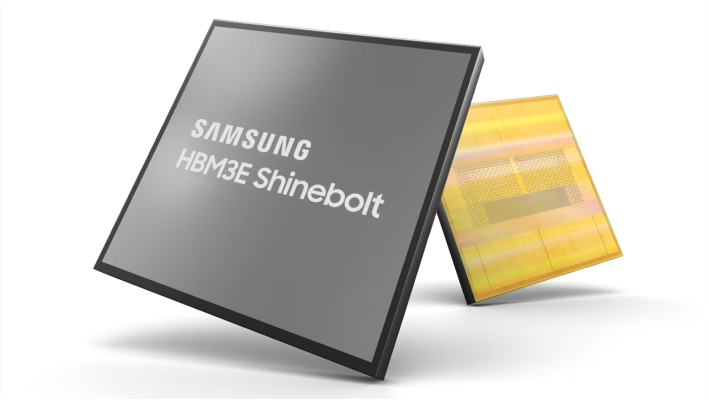
We're getting a first glimpses of Samsung's next-generation HBM3E and GDDR7 memory chips.
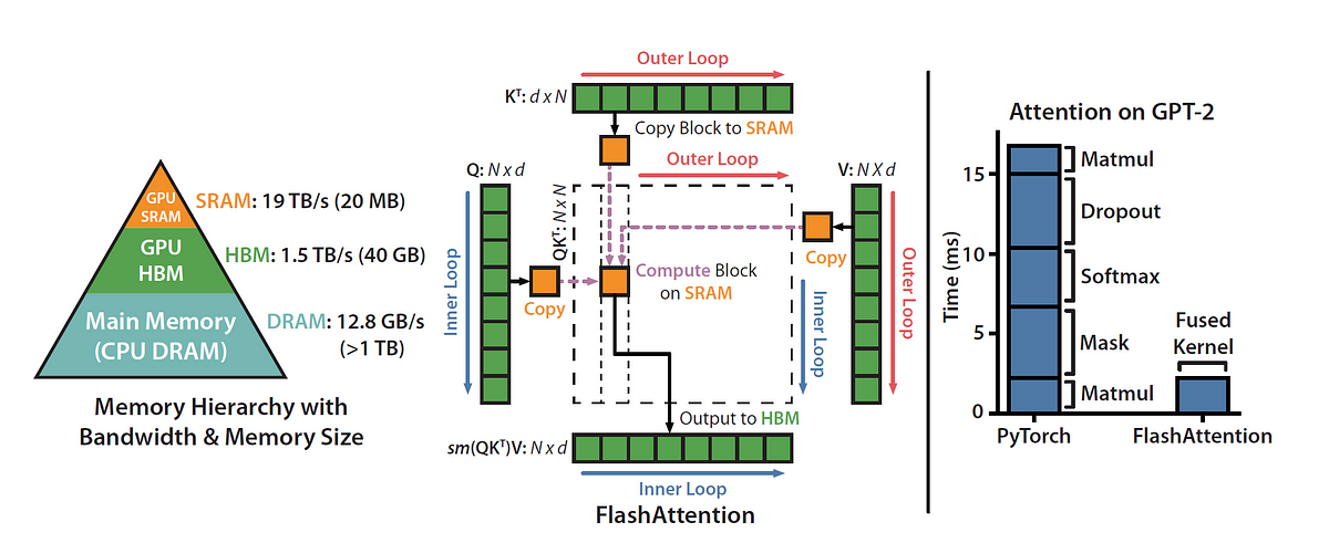
Step by step explanation of how one of the most important MLSys breakthroughs work — in gory detail.

tldr; techniques to speed up training and inference of LLMs to use large context window up to 100K input tokens during training and…
With the release of PyTorch 2.0 and ROCm 5.4, we are excited to announce that LLM training works out of the box on AMD MI250 accelerators with zero code changes and at high performance!
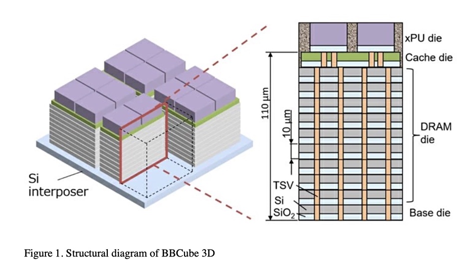
Tokyo Institute of Technology scientists have devised a 3D DRAM stack topped by a processor to provide four times more bandwidth than HBM.
Quarterly Ramp for Nvidia, Broadcom, Google, AMD, AMD Embedded (Xilinx), Amazon, Marvell, Microsoft, Alchip, Alibaba T-Head, ZTE Sanechips, Samsung, Micron, and SK Hynix
Micron $MU looks very weak in AI

We asked memory semiconductor industry analyst Jim Handy of Objective Analysis how he views 3D DRAM technology.
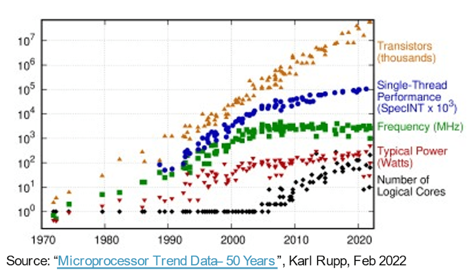
In the march to more capable, faster, smaller, and lower…
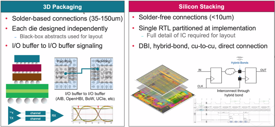
While terms often are used interchangeably, they are very different technologies with different challenges.
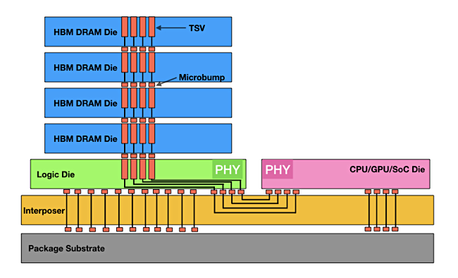
New applications require a deep understanding of the tradeoffs for different types of DRAM.
List of awesome open source hardware tools, generators, and reusable designs - aolofsson/awesome-opensource-hardware
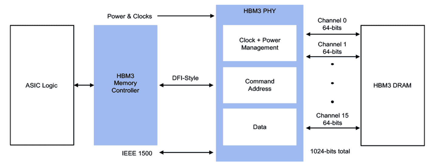
Changes are steady in the memory hierarchy, but how and where that memory is accessed is having a big impact.

Playing with reality

It's not clear when this mysterious memory will arrive, but SK Hynix is certainly talking a big game.
Increased transistor density and utilization are creating memory performance issues.

Let's learn more about the world's most important manufactured product. Meaningful insight, timely analysis, and an occasional investment idea.
There are two types of packaging that represent the future of computing, and both will have validity in certain domains: Wafer scale integration and
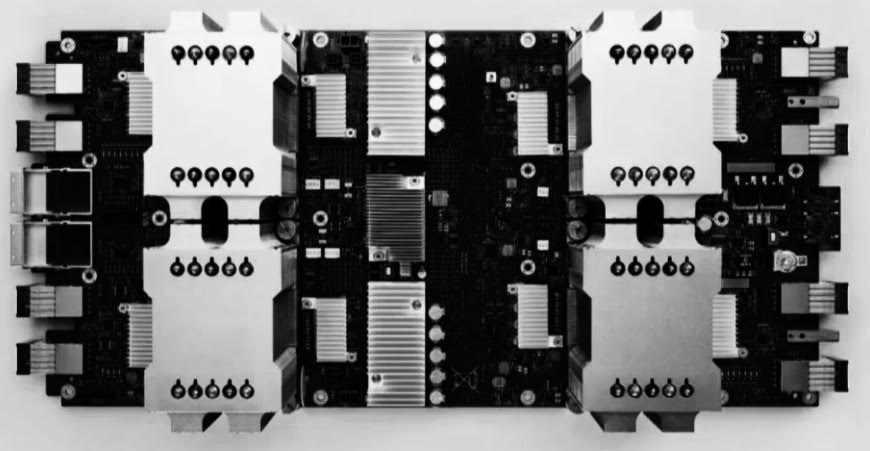
Google did its best to impress this week at its annual IO conference. While Google rolled out a bunch of benchmarks that were run on its current Cloud TPU
Explore Synopsys Blog for the latest insights and trends in EDA, IP, and Systems Design. Stay updated with expert articles and industry news.
This is a list of interface bit rates, is a measure of information transfer rates, or digital bandwidth capacity, at which digital interfaces in a computer or network can communicate over various kinds of buses and channels. The distinction can be arbitrary between a computer…

Experts at the Table: Which type of DRAM is best for different applications, and why performance and power can vary so much.
Over the last two years, there has been a push for novel architectures to feed the needs of machine learning and more specifically, deep neural networks.

Like its U.S. counterpart, Google, Baidu has made significant investments to build robust, large-scale systems to support global advertising programs. As
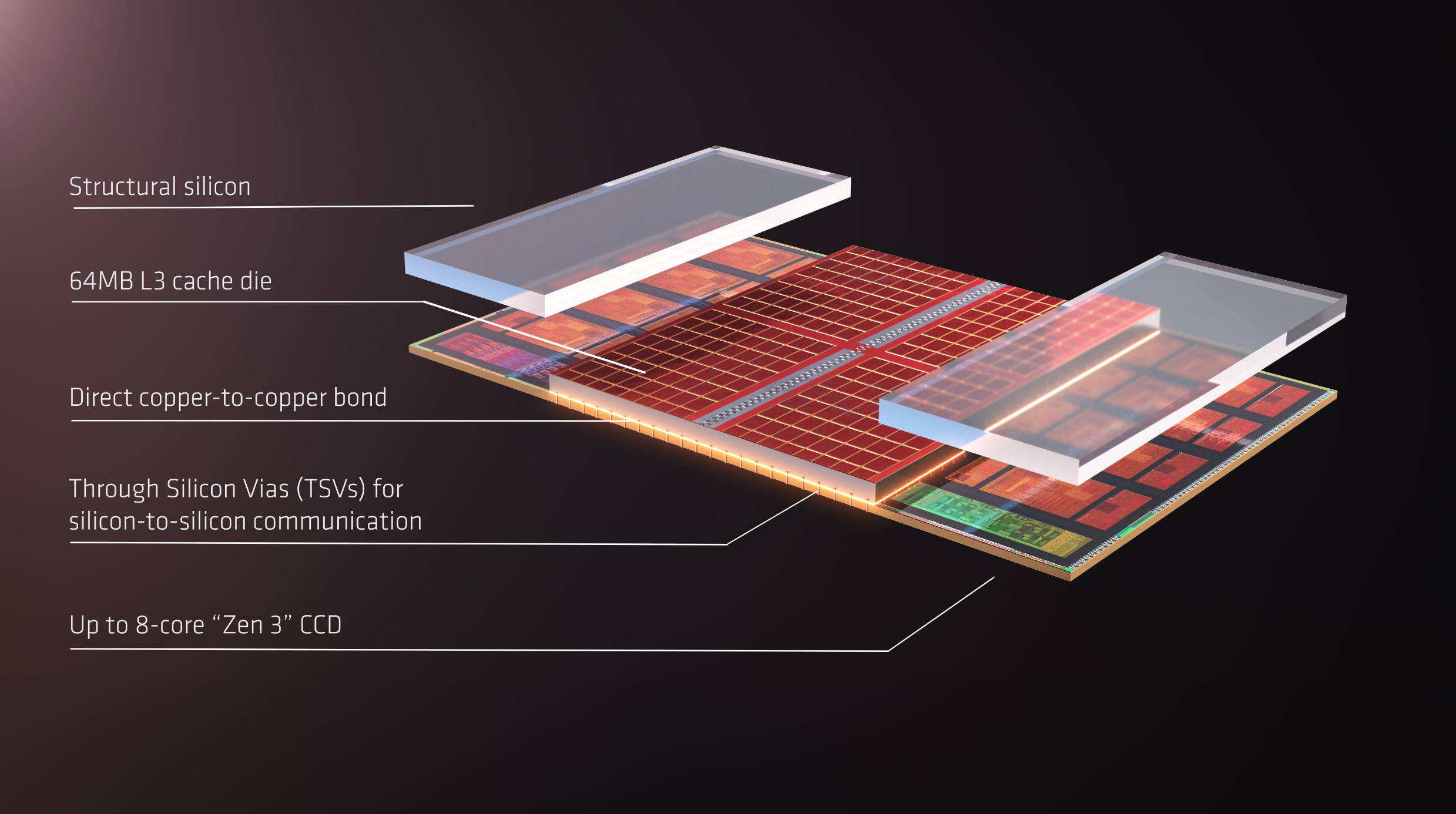
New interconnects offer speed improvements, but tradeoffs include higher cost, complexity, and new manufacturing challenges.

Sapphire Rapids, Intel's next server architecture, looks like a large leap over the just-launched Ice Lake SP.
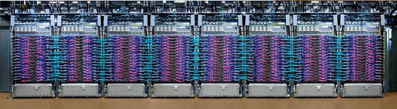
The inception of Google’s effort to build its own AI chips is quite well known by now but in the interests of review, we’ll note that as early 2013 the

Engineers must keep pace with advanced IC packaging technology as it evolves rapidly, starting with understanding the basic terms.
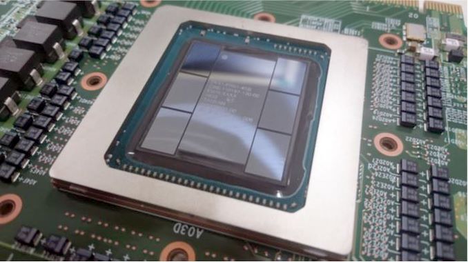
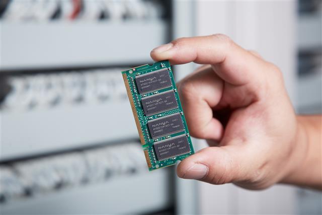
China-based DRAM chipmaker ChangXin Memory Technologies (CXMT) is scaling up its 19nm chip output with better yield rates, with the monthly production likely to top 70,000 wafers by the end of 2020, according to industry sources.
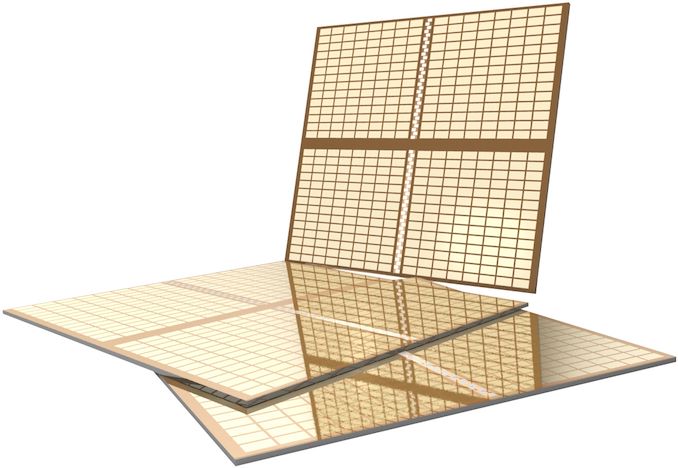
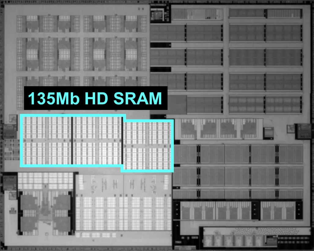
TSMC details its 5-nanometer node for mobile and HPC applications. The process features the industry's highest density transistors with a high-mobility channel and highest-density SRAM cells.
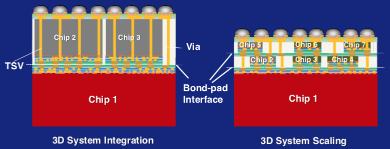
A dizzying array of choices and options pave the way for the next phase of scaling.

Why Chips Die Semiconductor devices face many hazards before and after manufacturing that can cause them to fail prematurely.

Processing In Memory Growing volume of data and limited improvements in performance create new opportunities for approaches that never got off the ground.
Google did its best to impress this week at its annual IO conference. While Google rolled out a bunch of benchmarks that were run on its current Cloud TPU
eBook: Nearly everything you need to know about memory, including detailed explanations of the different types of memory; how and where these are used today; what's changing, which memories are successful and which ones might be in the future; and the limitations of each memory…
A new crop of applications is driving the market along some unexpected routes, in some cases bypassing the processor as the landmark for performance and