The Tragedy of 3D XPoint (AKA Intel Optane AKA Micron QuantX)
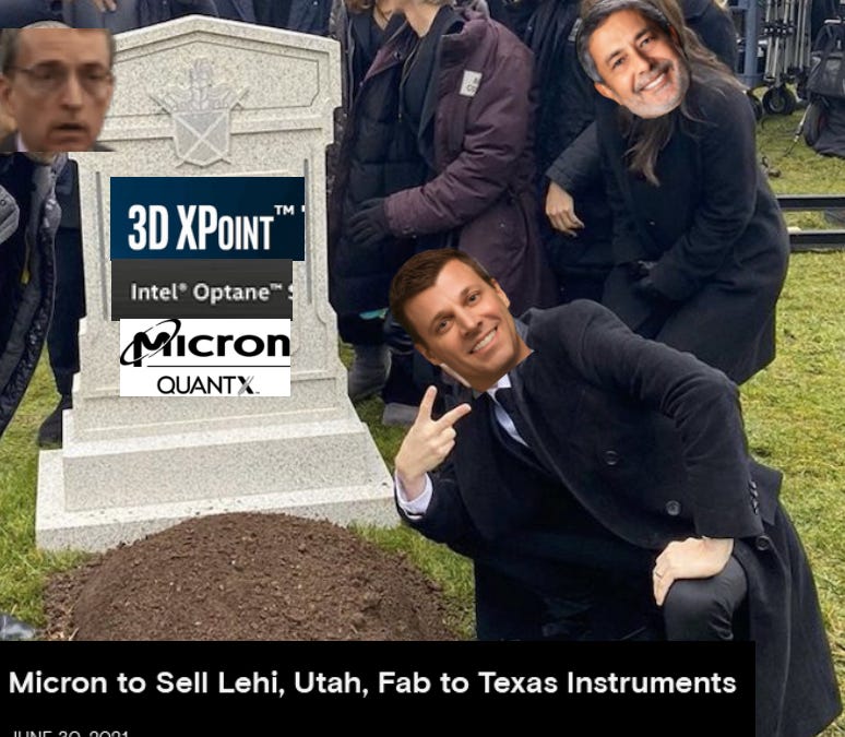
Too early and too late. Can it be resurrected from the dead?
Too early and too late. Can it be resurrected from the dead?
Dispatching, finite-capacity scheduling, MES, APC and simulation each attack a different share of the time wafers spend waiting, and all of them depend on accurate WIP and equipment-state data.
We are sharing two candidate magnets for next-generation computer memory, found by a team of Claude Opus 5.5 agents. Both are predicted to have zero net magnetism yet still sort electrons by spin: one a new compound we designed, the other a material first made in 1999. We're…

Complementary FETs (CFETs) extend nanosheet FET (NSFET) scaling by vertically stacking n- and p-type gate-all-around (GAA) devices, thereby shrinking standard-cell area. The performance gain, however, cannot be assessed from device metrics alone, as CFET layouts also introduce…
Note: Summary: This arXiv paper compares two next-generation chip technologies — A7 CFET and A10 NSFET — using a physics-based evaluation flow spanning from cell parasitics up to full-chip reliability. Approach: CFETs stack n- and p-type devices vertically to shrink cell area, but add extra cell-level resistance and capacitance. The authors built a flow linking calibrated device models, standard-cell…

Today’s tidal wave of queries is forcing hardware makers to pivot
Note: ### The AI Inference Revolution Is Here [IEEE Spectrum article](#rid:1854764141) — a survey of how the shift from AI training to AI **inference** is reshaping chip and memory design. **The shift** Since 2020, the AI story was about training ever-bigger models. In 2026 the spotlight has moved to inference — putting trained models to work. People actually use LLMs now, reasoning models run…

AI drastically shortened its design time; it will only get faster

Kepler Computing claims a new approach to chip design—and a proprietary material—can help end the supply bottlenecks that have sent memory prices surging.

How design-aware monitor analytics connects production measurements with device behavior and pre-silicon expectations.

Just because a chip is deemed good doesn't mean it will work as expected.
From Huawei's Ascend to a wave of GPU startups — thirteen companies racing to replace Nvidia
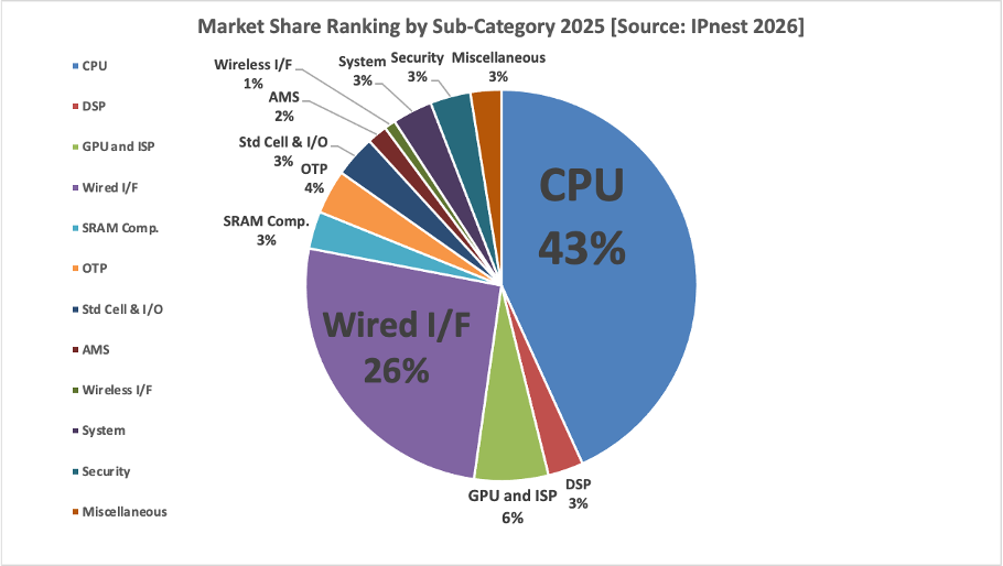
The $9.45 billion global design IP budget is distributed across 12 distinct sub-categories, heavily dominated by two primary pillars: CPU...

d-Matrix is tackling the 3D DRAM heat problem by stacking memory beneath the XPU, but atomic-level flatness remains a brutal barrier.

OpenAI revealed first benchmarks for its Jalapeño ASIC, showing up to 1.9× perf/W gains over existing hardware for LLM inference.
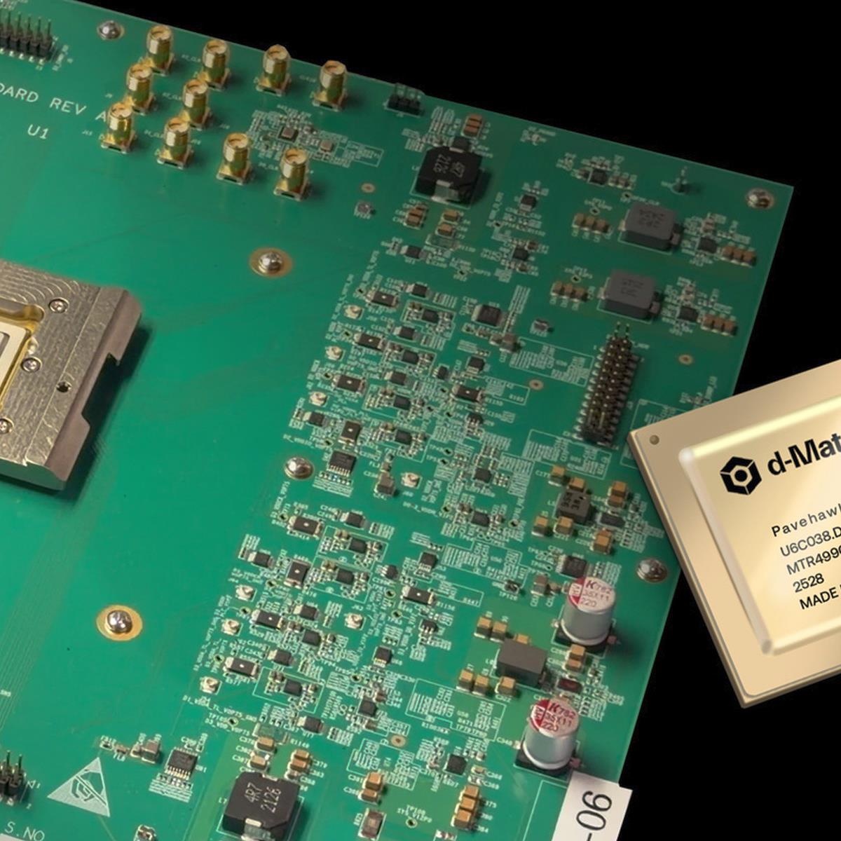
The company's ideas aren't novel, but it has solved long-standing challenges with 3D DRAM technology.
A look at AI Chip Architectures. NVIDIA, AMD, TPUs, Trainium, Groq, Cerebras.
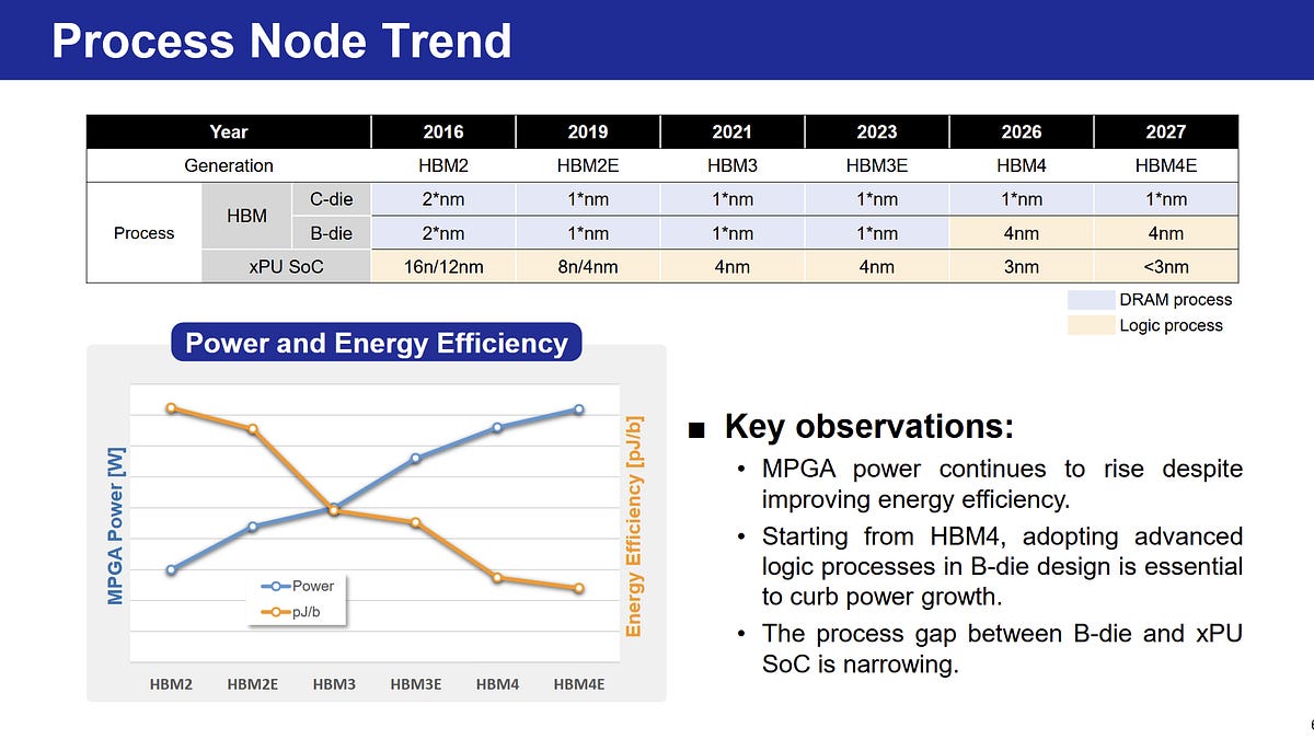
Machine learning applications demand ever more memory capacity and bandwidth. Samsung responded by fabricating their HBM base dies on a logic node, which opens up more opportunities
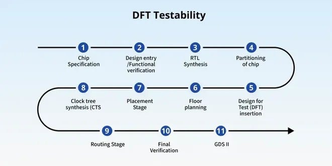
Designing a semiconductor chip is not only about making it perform its intended function.
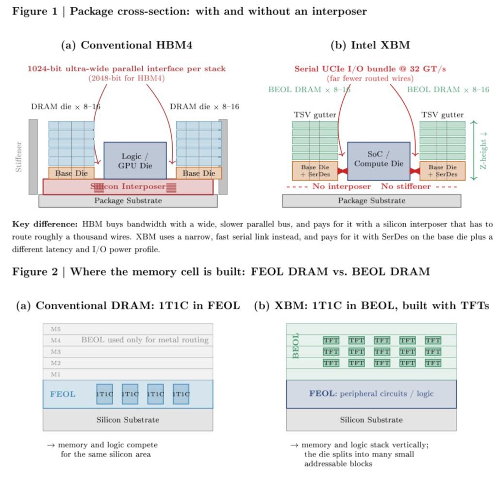
The most expensive part of HBM is not the DRAM. It is the piece of silicon underneath it. HBM moves data over a very wide parallel bus, roughly 1024 bits per stack. Every one of those wires has to be routed through a silicon interposer sitting between the memory and the compute…

Three core technologies involving advanced packaging, chip interconnects, and thermal design enable high-performance semiconductor systems.
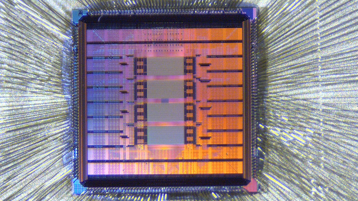
Sony will design the image sensors. The venture will use TSMC’s process
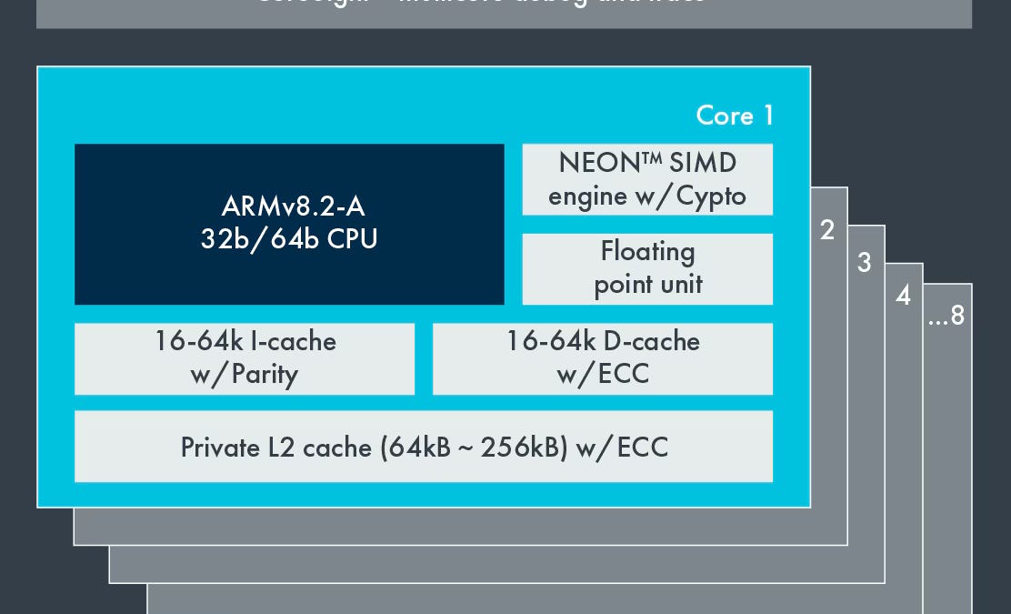
Arm’s 5-series cores are meant for tasks where performance barely matters, but power and area efficiency are top priorities.
As packages get larger and thinner, warpage is becoming a process-control problem rather than a simple flatness spec.

Cadence has announced that its AI-driven digital and custom reference flows, tools, and solutions are now Intel 18A-P & 14A certified.
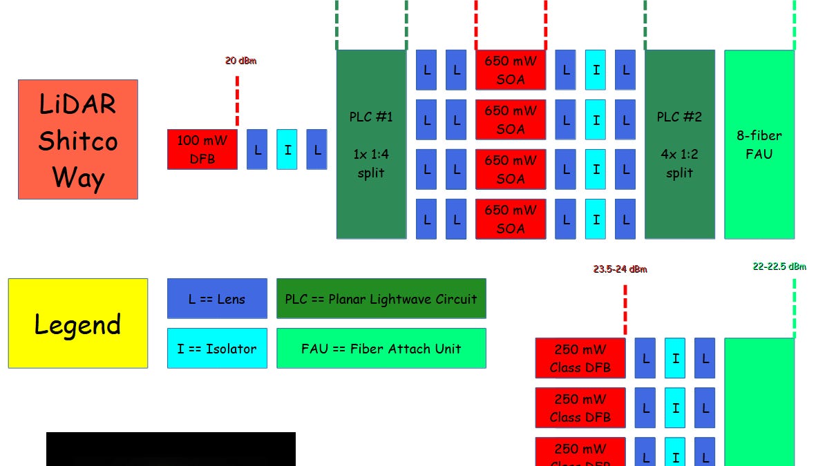
Degenerate stupid idea.
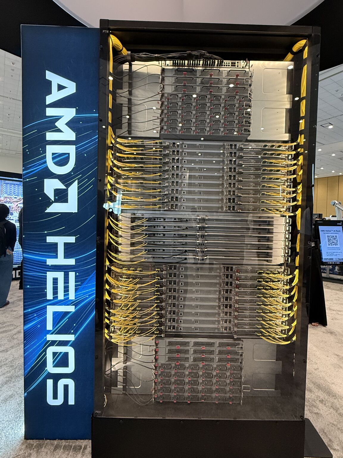
let's talk more technical details about AMD's Helios! Anthropic just signed a $5B deal with AMD. and AMD's own version of GTC, Advancing AI, is happening today and tomorrow. the high level details are: 72 MI455X GPUs, 432GB of HBM4 each, and 2.9 exaflops of FP4. but the most…
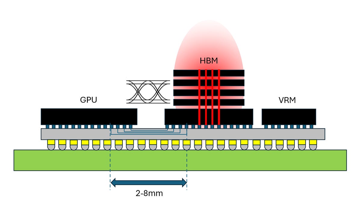
How transmission line effects and power-supply induced jitter make high-speed HBM interconnect scaling one of the most challenging co-design issues in AI racks

The unseen infrastructure of chipmaking
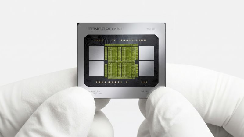
tensordyne just announced their chip specs. their trick is to turn every multiply into an add using logarithms, a trick from 1962 that everyone tried and gave up on. here's the breakdown: the idea is simple. log(a×b) = log(a) + log(b). store your numbers as logs and every…
Kioxia and Sandisk haVE started delivering samples of its tenth generation 3D NAND BiCS chips w ...
Note: RF design?
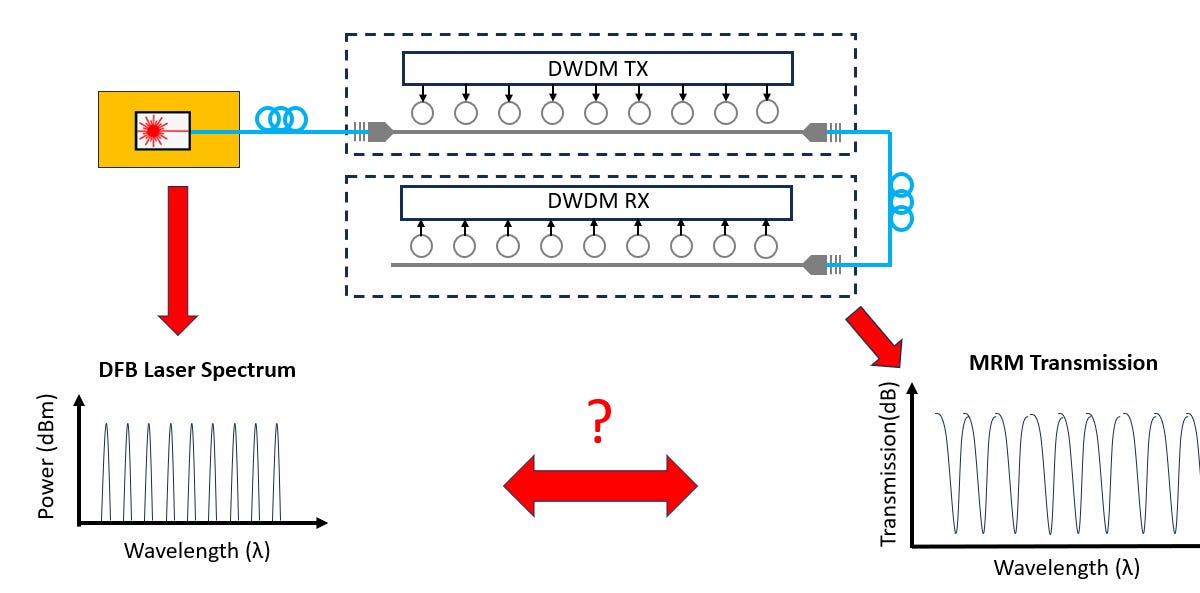
Key physics constraints and architecture challenges for scaling data rates in DWDM - ring modulator physics, clocking, CW-DFB Laser, and package integration
OpenAI and Broadcom introduce Jalapeño, a custom AI chip built for LLM inference to improve performance, efficiency, and scale across AI systems.

The AI era needs ever faster chips. ASML has a monopoly on the expensive contraptions needed to pattern them. Can anyone catch up?
Library of open source PDKs
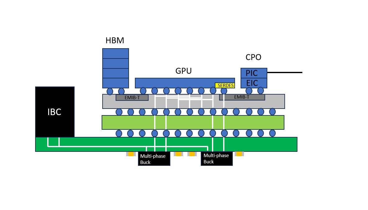
From 2D to 3.5D, a teardown of 2.5D CoWoS (TSV, RDL, Bump/pillar) and emerging trends (Glass, Panels, Bridges in Organic Substrate, and Hybrid Bonding)

NASA's High Performance Spaceflight Computing project aims to significantly enhance the computational capabilities of spacecraft, enabling autonomous operations and faster
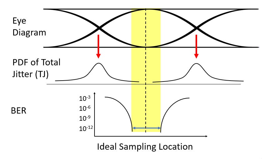
How signal integrity influences complexity of modern wireline transceiver architecture from first principles
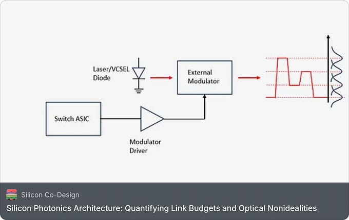
Silicon photonics is one of the hottest and fastest moving markets to address high speed data demands in co-packaged optics (CPO) in AI data centers. In this post I cover a few important high-level details to better understand silicon photonic circuits. These include: Link…

We’re only 7 years from the next evolution in transistors
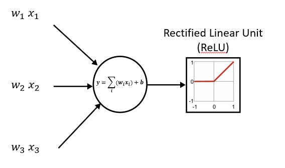
Learning from a classic AI accelerator - Eyeriss
Researchers at the University of Tokyo developed a magnetic switching device that operates at speeds up to 1,000 times faster
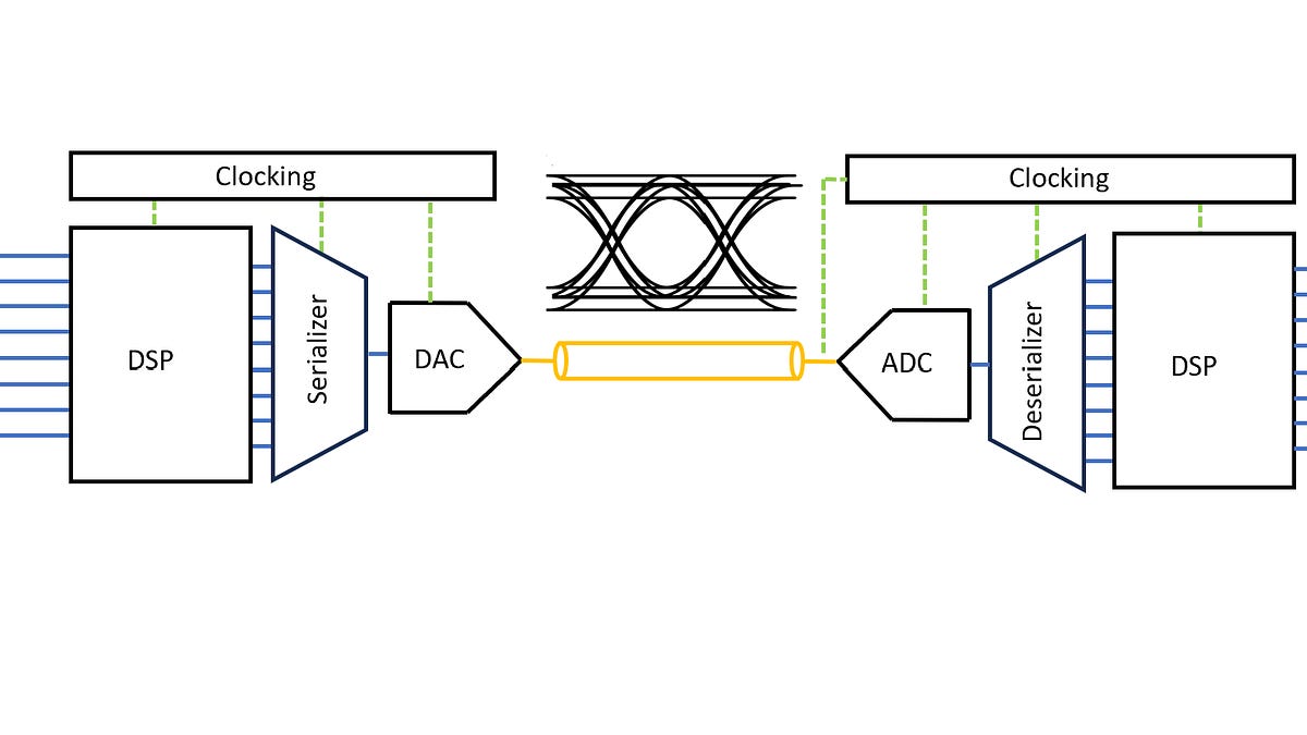
How high-speed data requirements influence chip architectural complexity

SiC vs GaN , HVDC, and the future of datacenter power.
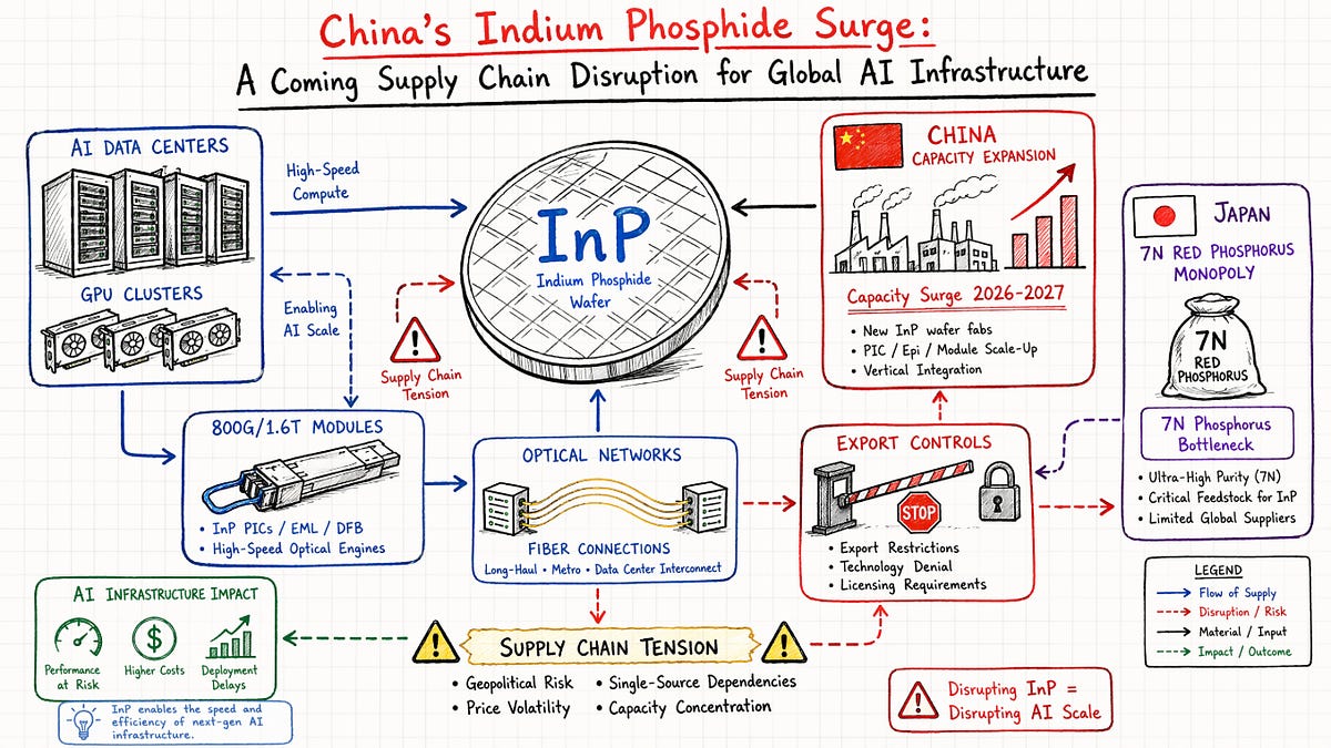
A Coming Supply Chain Disruption for Global AI Infrastructure
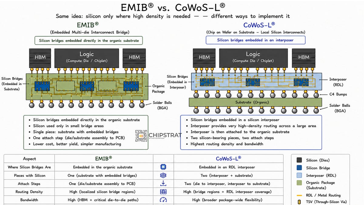
Is Intel's EMIB better than TSMC's CoWoS for AI accelerators? A primer on both, an honest look at the trade-offs, and where it goes from here.
Laying the Groundwork of the Current Chip Design Paradigm
file format used for specification of data structures for photomask production
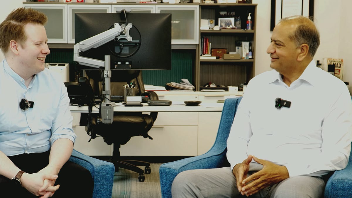
Q&A with SiTime CEO Rajesh Vashist