RF Engineering is Black Magic
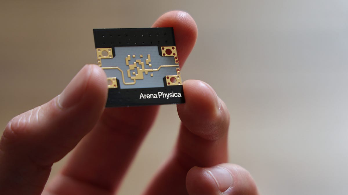
Tribal knowledge of RF design, EV range vs. temperature on the dyno, OpenAI's expanding robotic division, and more.
Tribal knowledge of RF design, EV range vs. temperature on the dyno, OpenAI's expanding robotic division, and more.
As Intel primes its 18A-P technology at external customers, the company is sharing new insights into its enhanced performance & features.
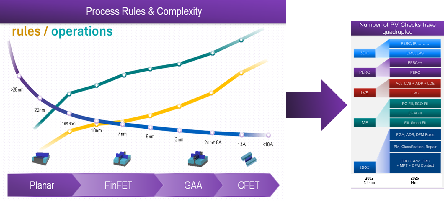
This blog looks at the details of how Synopsys IC Validator can overcome the advanced node physical verification bottleneck.
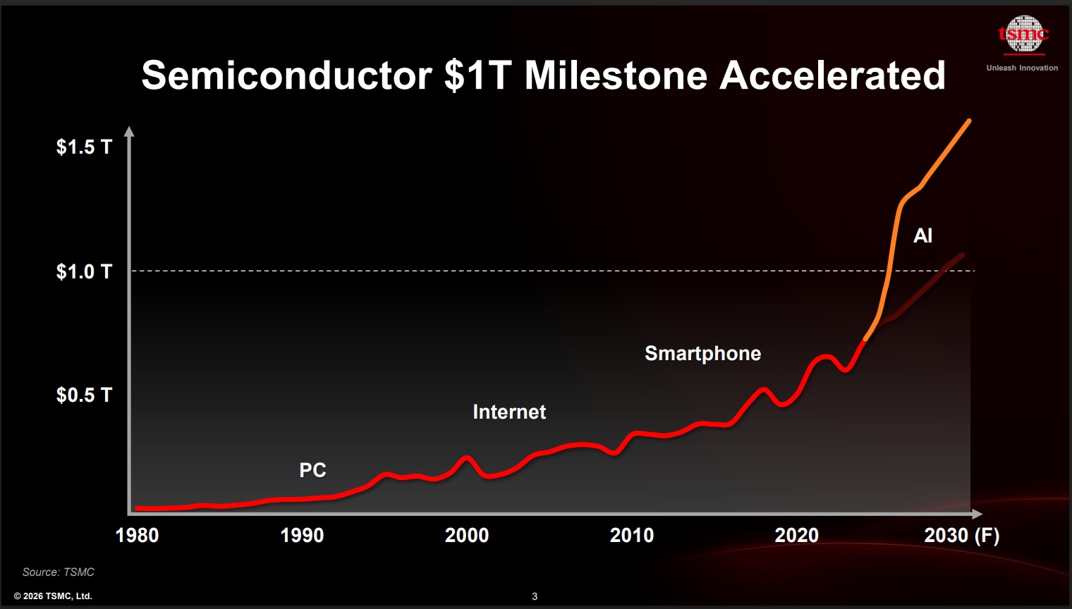
TSMC revenue is expected by me to grow 30-40%. Here is the hitch: While wafer pricing is stable chip pricing is not.

DRAM Market Shift: From Mobile to Infrastructure (2023–2030) The latest DRAM demand outlook highlights a clear structural transition: memory demand is moving from mobile-driven to infrastructure-driven growth. 1. Infrastructure Becomes Dominant Servers & Workstations grow from…

🚨 DDR4 / LPDDR4: The Beginning of the End — or a Strategic Reset? The memory industry is approaching a pivotal inflection point—and the signals are becoming impossible to ignore. Recent developments from Samsung indicate that legacy nodes such as LPDDR4 (and increasingly DDR4)…

Rambus has announced its LPDDR5X SOCAMM2 memory chipset, a vital component to enable the next-gen compact memory for AI datacenters.

Tenstorrent has previewed its optimized AI model, which is powered by the Blackhole servers, offering blazing-fast video generation speeds.
The cost case is strengthening, but glass, warpage, and bonding yield stand in the way.

Google is preparing two brand new chips under its TPUv8 belt, one for training & one for inference AI workloads.

AMD's 3D V-Cache CPUs deliver a huge boost versus the Non-X3D part in AI benchmarks, showcasing why they are best suited for RAG pipelines.
But LLMs' limitations can be seen when it needs to generate responses on data it wasn't trained on.
That's where RAG or Retrieval-Augmented Generation) comes into play

The U.S.-Israeli war with Iran, now in an unstable ceasefire, has exposed a structural failure in the global semiconductor memory supply chain, and it is

A new embedded memory architecture with a three-transistor cell.

The startup's programmable chip uses a metasurface architecture to control light without moving parts.
Himax Technologies has long been seen as a peripheral player in the AI boom. But that perception may be about to change. Buried inside a series of recent TSMC patent filings lies an unexpected...

Lace, a Norway-headquartered chipmaking equipment startup which is backed by Microsoft, has raised $40 million in funding to further develop a technology that could enable significant advances in semiconductor design and manufacturing, the company said on Monday.
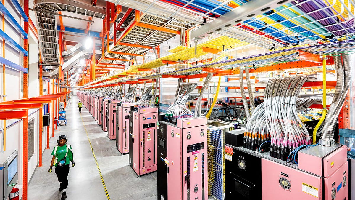
Why Anthropic’s integration into hyperscaler silicon programs may give it a lasting advantage in the economics of frontier AI.

Shortly after Amazon announced its $50 billion investment in OpenAI, AWS invited me on a private tour of the chip lab at the heart of the deal.
Note: Based on the article **[An exclusive tour of Amazon’s Trainium lab, the chip that’s won over Anthropic, OpenAI, even Apple](#rid:1653401870)**, here are the key points: ### Strategic Impact & Partnerships * **Major Adoption:** Amazon’s custom chips have secured massive commitments from leading AI labs. **Anthropic** runs Claude on over 1 million Trainium2 chips, and **OpenAI** recently signed a…

TSMC N3 Wafer Shortages, Memory Constraints, Datacenter Bottlenecks, Supply Chain Wars Winner
Designing AI Chip Hardware and Software Bjarke Hammersholt Roune 2026 This document is, for now, open for comments. You can use the Google Docs comment feature to add comments anywhere. Thanks! What is this document? I was going to start an AI chip company and this document…

Space Forge's orbital furnace could redefine semiconductor production with space-grown crystals.

Explore the four key modern memory types: ROM, DRAM, SRAM, and flash, their unique roles, and trade-offs in speed, cost, and storage.

UC San Diego researchers have reimagined RRAM, creating a device that could redefine AI's memory challenges. Discover how this could impact edge computing.
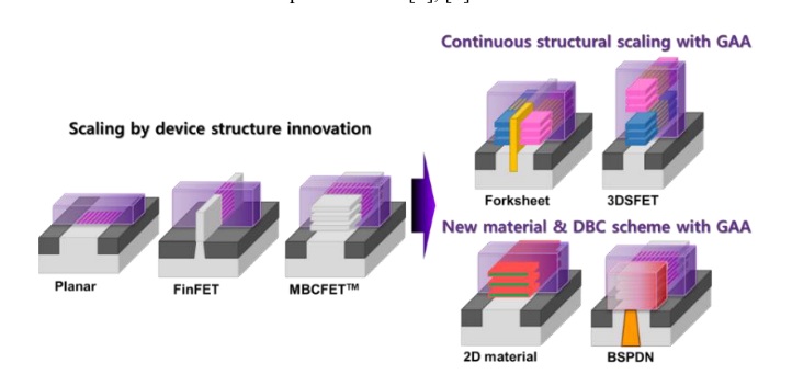
Key takeaways ▼ The transition from FinFET to Gate-All-Around (GAA) transistor technology represents a pivotal moment in the evolution of logic devices, driven by both physical scaling limits and the … Continue reading "Gate-All-Around (GAA) Technology for Sustainable AI"

Tighter process control and yield optimization still cannot mitigate crystalline defects.
In this article, we'll walk through the steps of generating a Process Design Kit (PDK) for digital standard cell libraries.
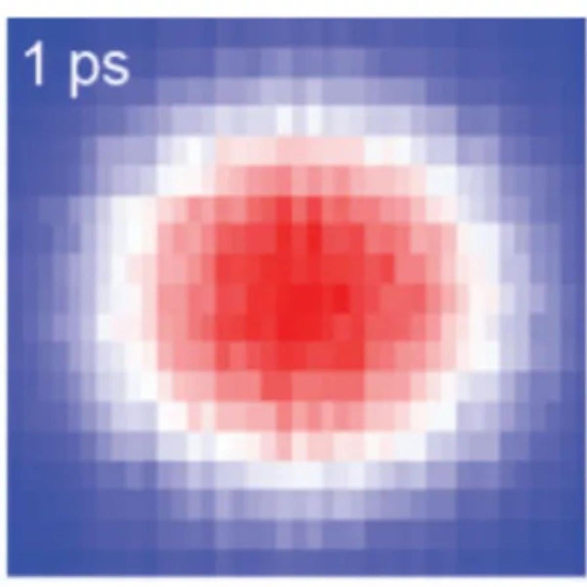
A multi-institution research team has discovered a metallic material that conducts heat nearly three times more efficiently than copper or silver.

IEDM 2025 Round-Up
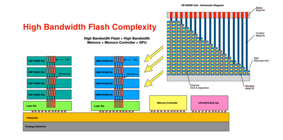
For leading fabs, this is a 3xx-layer 3D NAND process, which yields on the order of 20-30 Gb/mm2 of memory.
321-layer process has 44% more memory per wafer than the previous generation 238-layer technology

NVIDIA is formally announcing its Rubin AI platform today which will be the heart of next-gen Data Centers, with a 5x upgrade over Blackwell.
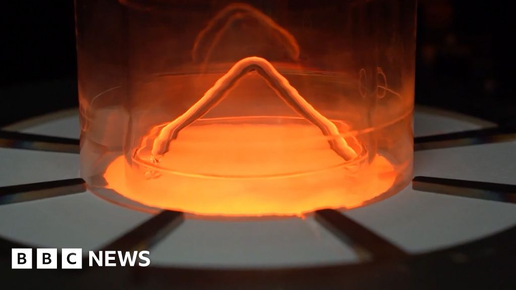
Just a handful of companies can make cadmium zinc telluride, a material with powerful properties.
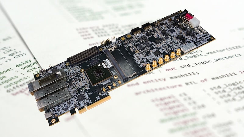
FPGAs are limited by outdated proprietary software. Learn how embracing open-source tools is necessary to modernize FPGA development and unlock their full potential.

Tech giants including Meta, Alphabet, Microsoft and Amazon have all extended the estimated useful lives of their servers and AI equipment over the past five years, sparking a debate among investors about whether these accounting changes are artificially inflating profits. Meta…
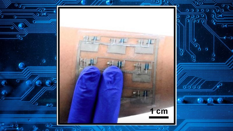
A new “rubbery CMOS” platform combines fully stretchable p- and n-type transistors, enabling skin-like logic circuits and a tactile “sensory skin” for wearables, implants, and soft robotics.

I've been studying the standard cell circuitry in the Intel 386 processor recently. The 386, introduced in 1985, was Intel's most complex pr...

Thin films for insulating different components are causing dissipation issues in advanced chips.
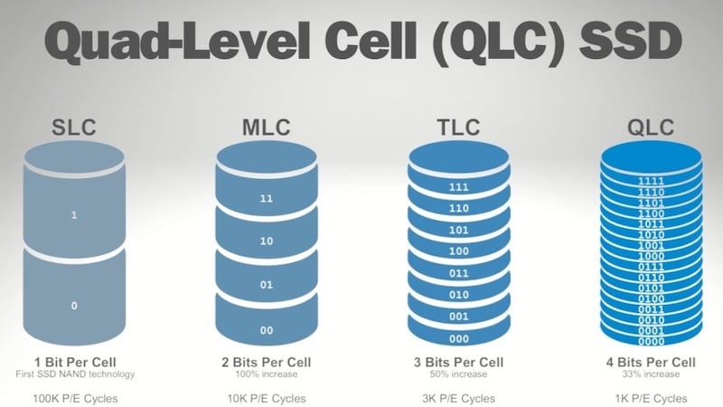
Learn how to solve QLC NAND's endurance, ECC, and performance issues for hyperscale. The approach blends a PCIe Gen5 controller with hardware-accelerated LDPC, PerformaShape QoS, and more.

Researchers focus on limiting data movement to reduce power and latency in edge devices.

Modeling, simulation, and digital twins enable EUV innovation.

Our selection of industry specific magazines cover a large range of topics.

Bump technologies are being pushed beyond what was thought to be their physical and performance limits.
The mechanism behind this is a time-resource matrix: A scheduling framework that orchestrates compute, memory and control resources across time. Much like a train timetable, scalar, vector and matrix operations move across a synchronized compute fabric without pipeline stalls or contention.
By predicting exactly when data will arrive — whether in 10 cycles or 200 — Deterministic Execution can slot dependent instructions into the right future cycle. This turns latency from a hazard into a schedulable event, keeping the execution units fully utilized and avoiding the massive thread and…
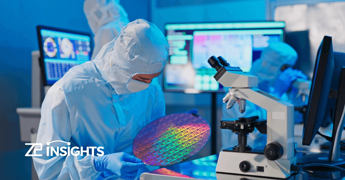
The semiconductor manufacturing landscape continues to grow, with new fabs and expansions to current production sites taking place in the U.S., Asia, and other key manufacturing regions.

The expanding role of GaN in power electronics. Gallium nitride (GaN) has emerged as one of the most disruptive semiconductor technologies of the decade, with a market projected to reach $3 billion by 2030. Consumer applications, particularly fast chargers, have been the early…
Timing is increasingly dependent on vectors. Can static techniques continue to deliver the necessary results? Maybe.

Memory latency, bandwidth, capacity, and energy increasingly limit performance. In this paper, we reconsider proposed system architectures that consist of huge (many-terabyte to petabyte scale) memories shared among large numbers of CPUs. We argue two practical engineering…
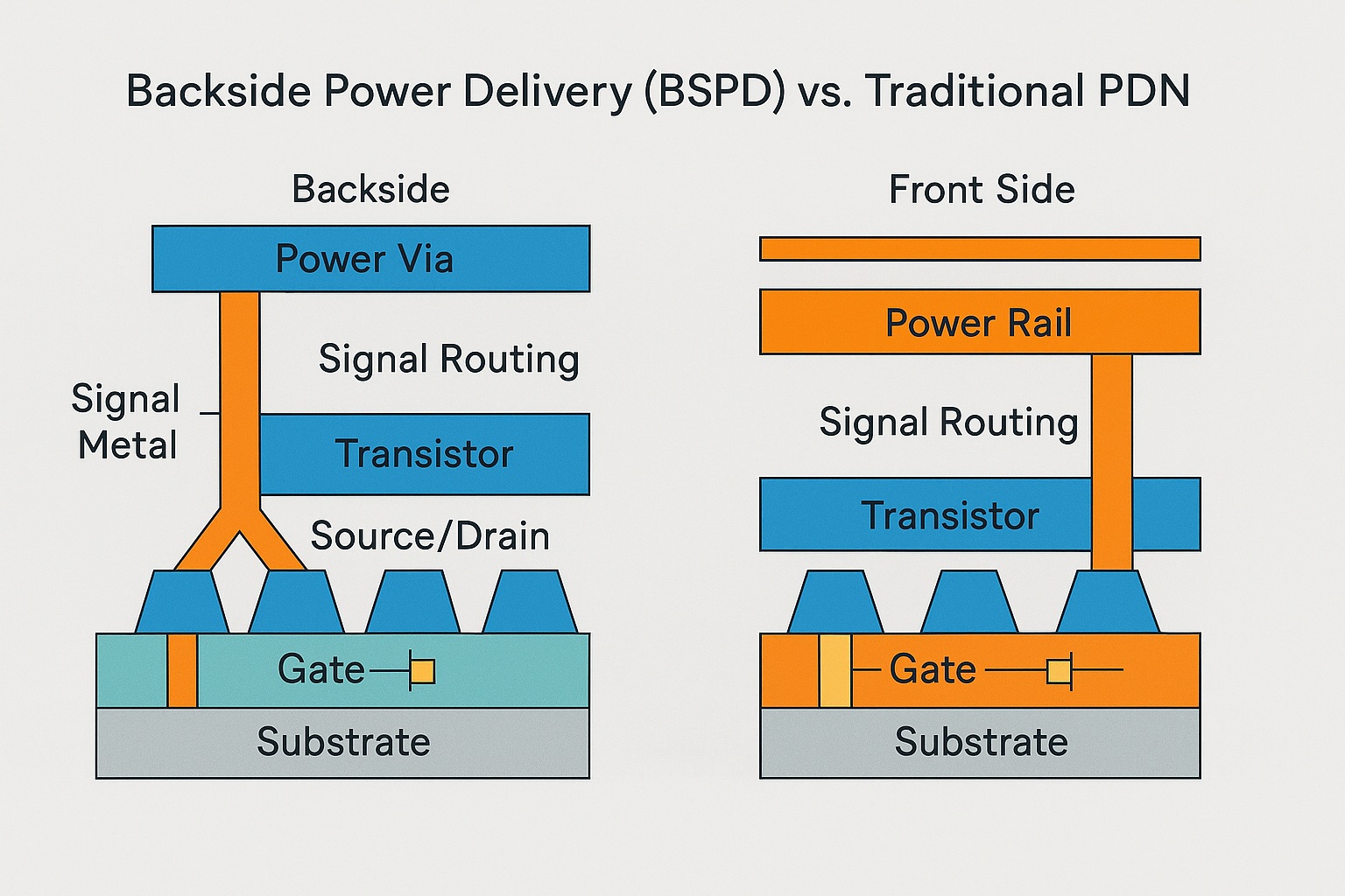
Backside Power Delivery (BSPD), also called Backside Power Delivery Network (BSPDN) or backside power via (BPV) technology, is a semiconductor manufacturing innovation in which the chip’s primary power distribution network … Continue reading "Backside Power Delivery (BSPD) Wiki"

A new technical paper titled “Energy-Accuracy Trade-Offs in Massive MIMO Signal Detection Using SRAM-Based In-Memory Computing” was published by researchers at the University of Illinois at Urbana–Champaign. Abstract “This paper investigates the use of SRAM-based in-memory…
Note: “This paper investigates the use of SRAM-based in-memory computing (IMC) architectures for designing energy efficient and accurate signal detectors for massive multi-input multi-output (MIMO) systems. SRAM-based IMCs are the state-of-the-art for executing deep learning workloads in terms of energy efficiency and compute density. However, given the more stringent accuracy requirements of massive…

Materials breakthroughs and process innovations are unlocking next-gen chip scaling, with Southeast Asia playing a pivotal role in semiconductor evolution. By Andrew Goh, Corporate Vice President and General Manager, Southeast Asia at Lam Research
Tungsten, long used for interconnects due to its robustness and thermal stability, is now reaching critical scaling and performance bottlenecks. Its relatively high resistivity and poor conformality in narrow, high-aspect-ratio features
he industry is turning to molybdenum (Mo) as a breakthrough alternative. Mo offers lower resistivity, enabling faster electron flow and reduced power consumption, which are crucial for maintaining performance at smaller nodes. Its ability to be deposited without a barrier layer simplifies…