NVIDIA Unveils NVHBM Memory To Turbocharge AI Chip Speeds By 30%
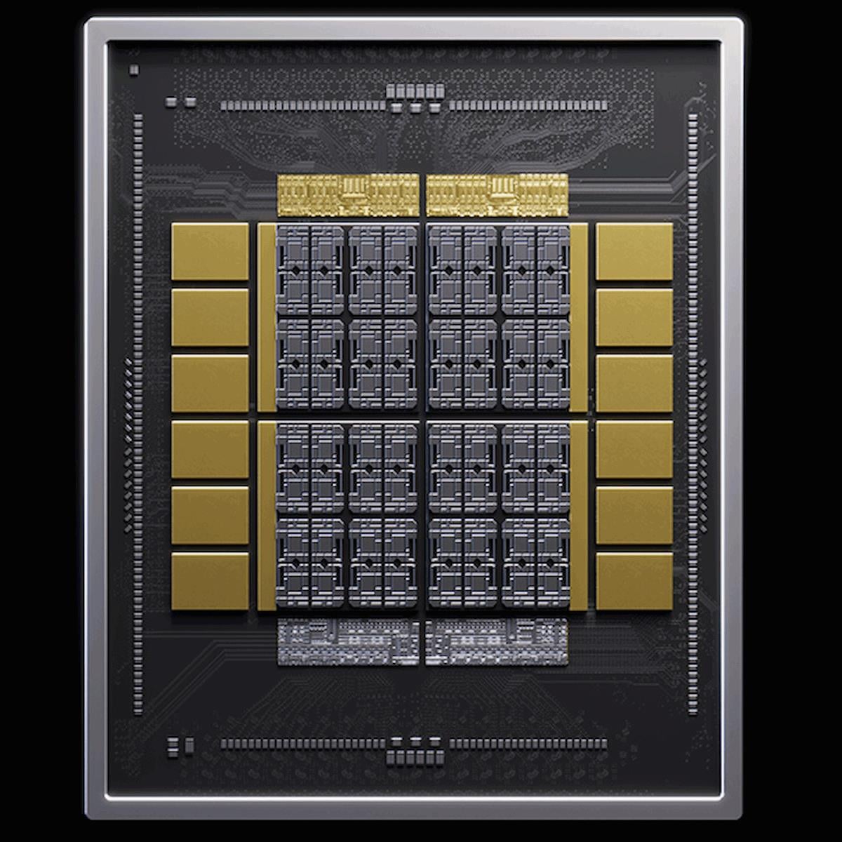
NVIDIA's NVHBM is a new memory technology that partners can license, offering improved efficiency and performance over standard HBM.
NVIDIA's NVHBM is a new memory technology that partners can license, offering improved efficiency and performance over standard HBM.
A look at AI Chip Architectures. NVIDIA, AMD, TPUs, Trainium, Groq, Cerebras.
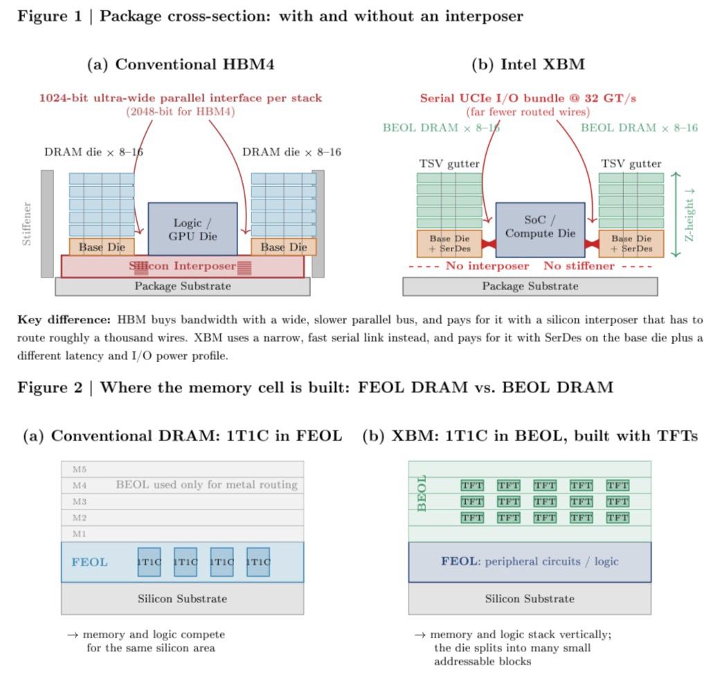
The most expensive part of HBM is not the DRAM. It is the piece of silicon underneath it. HBM moves data over a very wide parallel bus, roughly 1024 bits per stack. Every one of those wires has to be routed through a silicon interposer sitting between the memory and the compute…

Three core technologies involving advanced packaging, chip interconnects, and thermal design enable high-performance semiconductor systems.
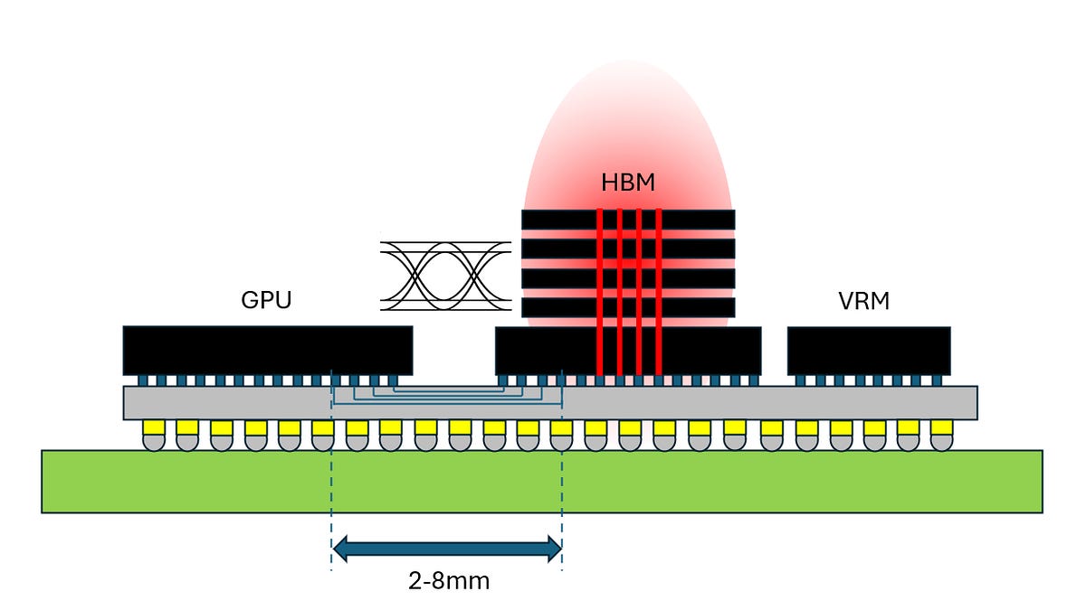
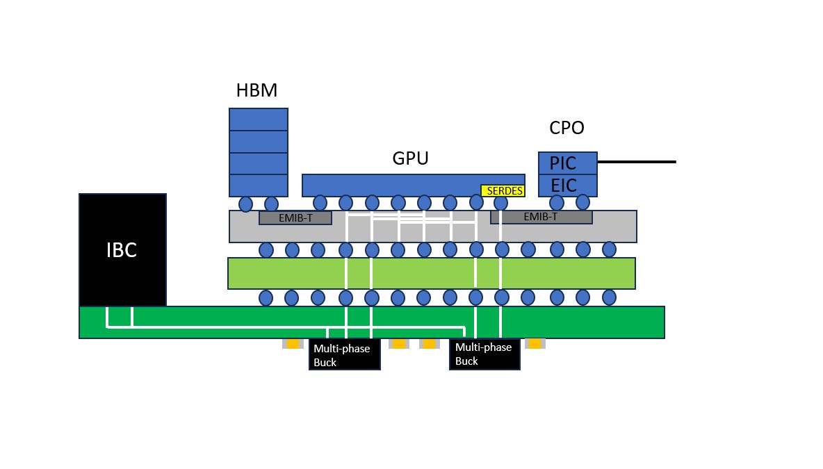
How transmission line effects and power-supply induced jitter make high-speed HBM interconnect scaling one of the most challenging co-design issues in AI racks

Read this blog to learn what PCI Express is, how PCIe 7.0 improves bandwidth and efficiency, and how features like PAM4, FEC, FLIT mode and AXI support next-generation AI, cloud, HPC and edge systems.

It has been nine years since a Chinese HPC supercomputer was at the top of the High Performance Linp ...
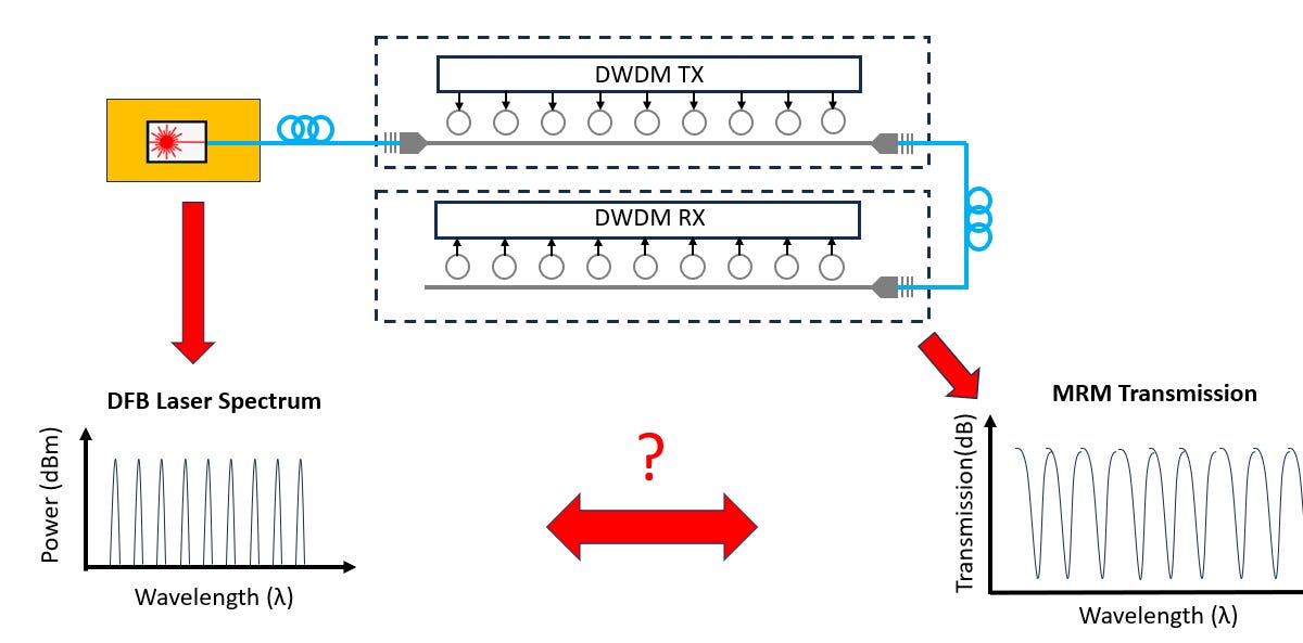
Key physics constraints and architecture challenges for scaling data rates in DWDM - ring modulator physics, clocking, CW-DFB Laser, and package integration
From 2D to 3.5D, a teardown of 2.5D CoWoS (TSV, RDL, Bump/pillar) and emerging trends (Glass, Panels, Bridges in Organic Substrate, and Hybrid Bonding)
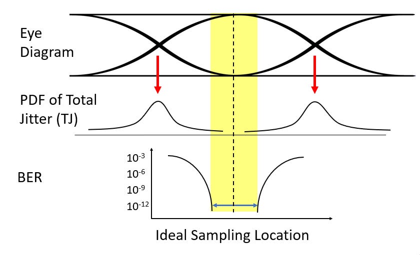
How signal integrity influences complexity of modern wireline transceiver architecture from first principles
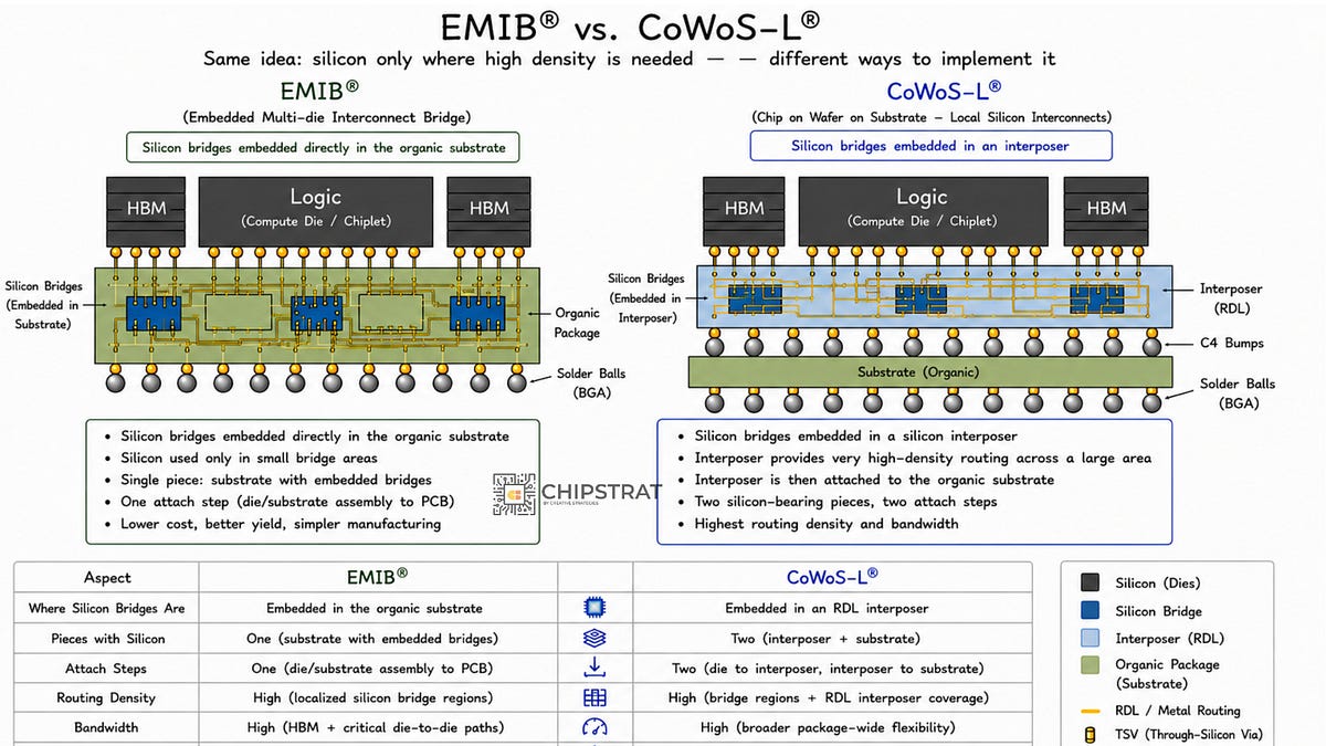
Is Intel's EMIB better than TSMC's CoWoS for AI accelerators? A primer on both, an honest look at the trade-offs, and where it goes from here.

IEDM 2025 Round-Up
For leading fabs, this is a 3xx-layer 3D NAND process, which yields on the order of 20-30 Gb/mm2 of memory.
321-layer process has 44% more memory per wafer than the previous generation 238-layer technology

Co-Packaged Optics (CPO) has long promised to transform datacenter connectivity, but it has taken a long time for the technology to come to market, with tangible deployment-ready products only arriving in 2025.
copper-based scale-up solutions, such as NVLink, provide tremendous bandwidth of 7.2 Tbit/s per GPU – soon to be 14.4 Tbit/s per GPU in the Rubin generation, yet copper-based links are limited in range to two meters
Rubin

Bump technologies are being pushed beyond what was thought to be their physical and performance limits.

A 94-page research report on interconnect fundamentals for semiconductor engineers.

The NVIDIA Collective Communication Library (NCCL) is a critical software layer enabling high-performance collectives on large-scale GPU clusters. Despite being open source with a documented API, i…

Thin lines and limited ground planes keep RDL interconnects short.

CXL 3.1 and PCIe 6.2 are transforming AI with improved data transfer and memory pooling.

Many features of UCIe 2.0 seen as “heavy” are optional, causing confusion.
The spec is defined with so many variants that you can tailor it to your exact needs. It’s applicable for everything from automotive to high-performance compute to AI to mil/aero because it has so many flavors. That’s also a curse to an IP provider. How do you support all those flavors?”
the latter predominates, since virtually all projects underway are internal projects, with all chiplets being internally created and applied. Interoperability with externally sourced chiplets is therefore not a concern
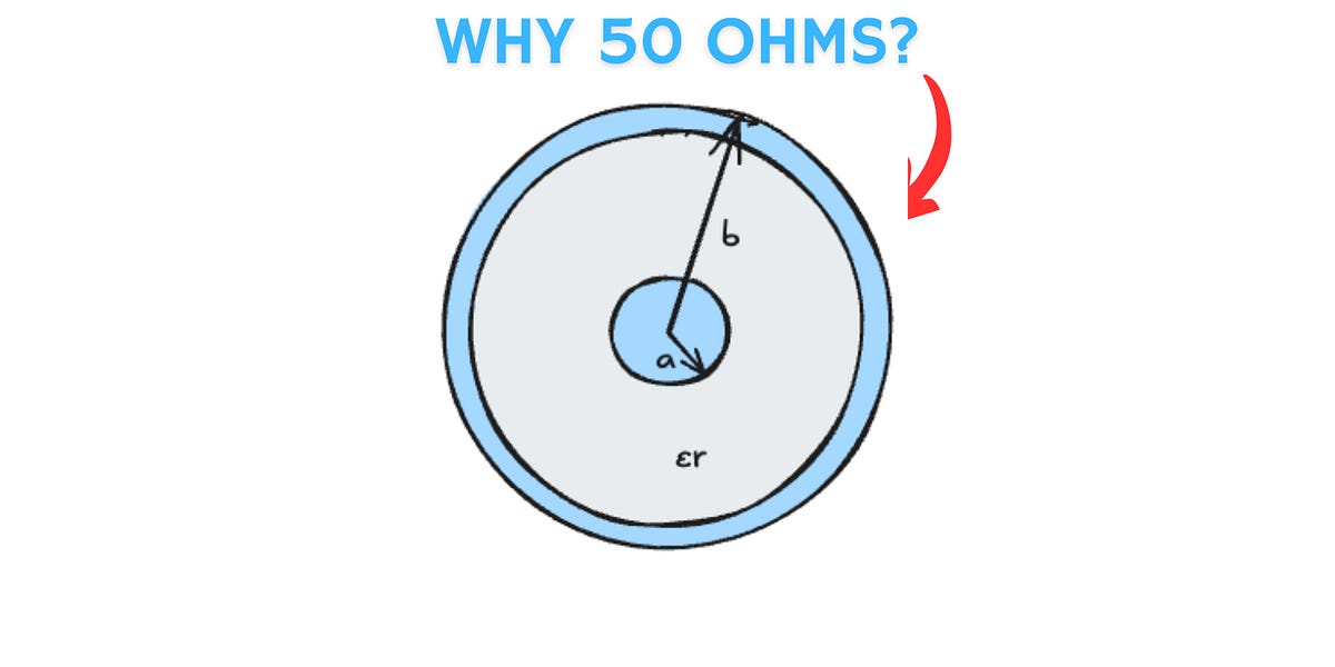
The history, physics, and practical trade-offs behind a number every RF engineer knows.
One of the fundamental properties of a coaxial cable is its characteristic impedance often represented by Z0. It is the value of resistance seen when looking into a coaxial cable of infinite length. The value of Z0 is solely determined by the physical construction of the cable.
air-filled (εr=1),
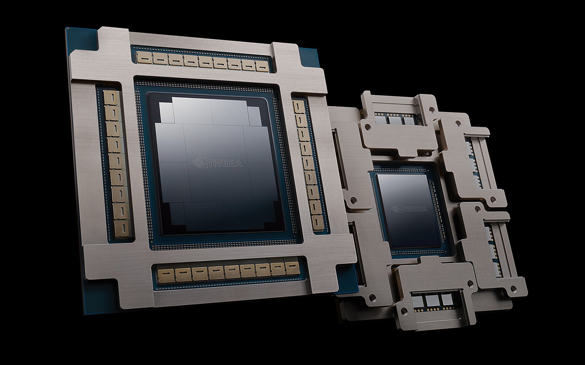
Nvidia's endorsement of co-packaged optics means the time is right

Understanding and minimizing discontinuities is increasingly important as serial links become both shorter and faster. Applying the old edge rate to roundtrip relationship to the modern era, Donald Telian in this article offers a rule-of-thumb to help gauge which interconnect…
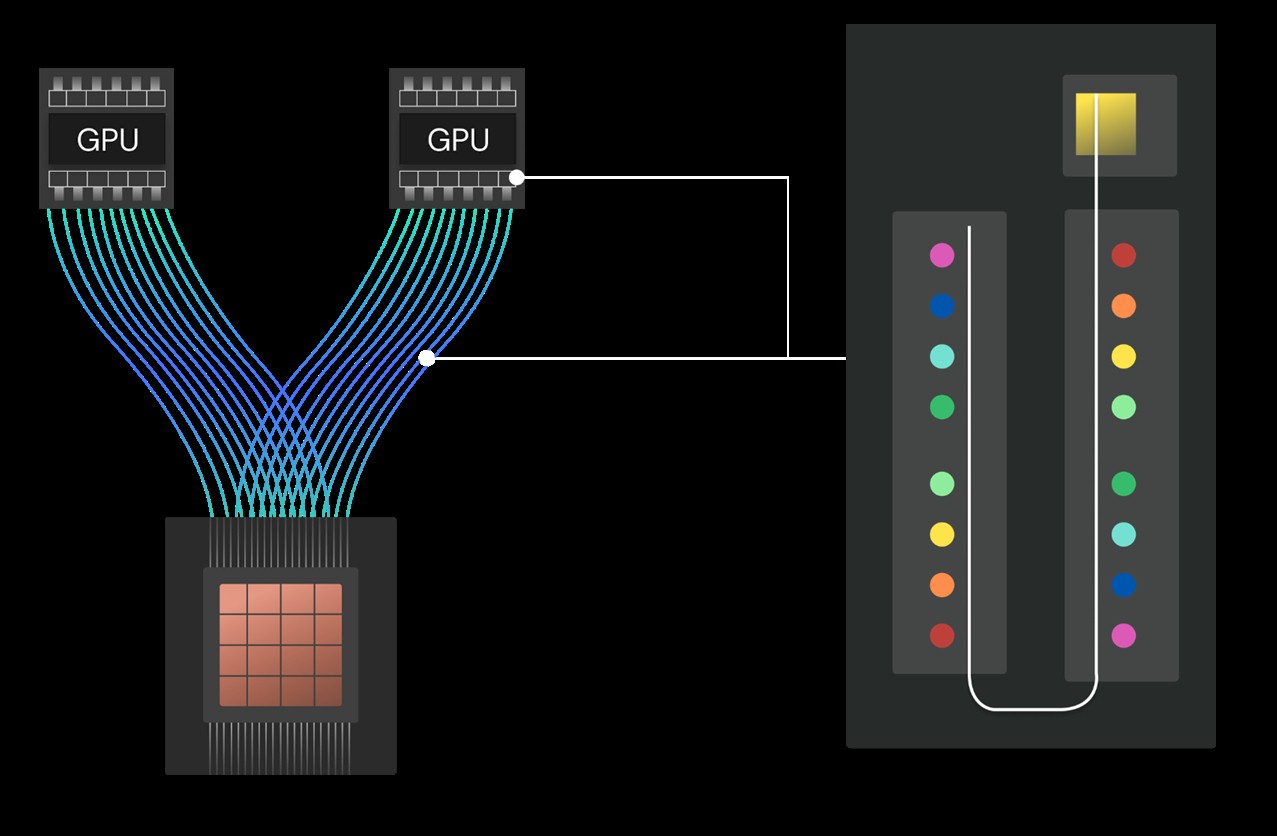
According to rumors, Nvidia is not expected to deliver optical interconnects for its GPU memory-lashing NVLink protocol until the “Rubin Ultra” GPU
According to rumors, Nvidia is not expected to deliver optical interconnects for its GPU memory-lashing NVLink protocol until the “Rubin Ultra” GPU
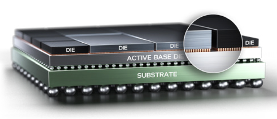
Foundry competition heats up in three dimensions and with novel technologies as planar scaling benefits diminish.
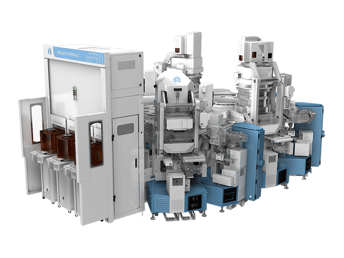
In this guide, we’ll elucidate the pivotal role of FO-PLP in advancing the semiconductor sector. Harnessing cost-effectiveness with enhanced functionality, FO-PLP beckons a new era of electronic sophistication. Let’s delve into the ultimate guide to Fan-Out Panel-Level Packaging…
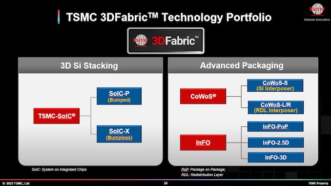
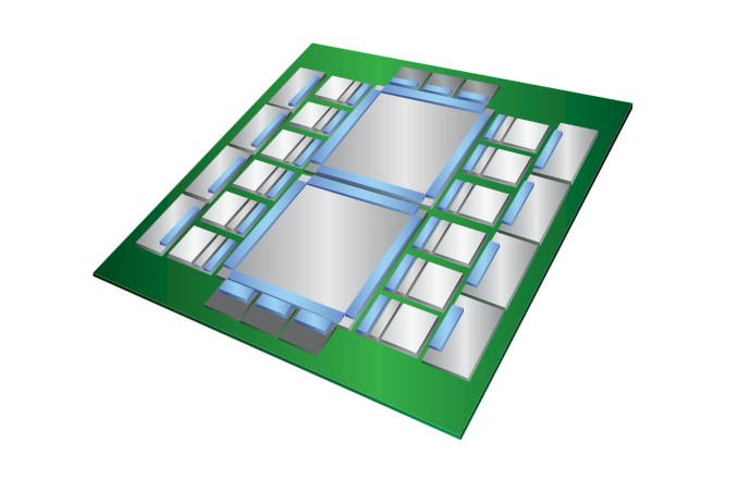
While a lot of people focus on the floating point and integer processing architectures of various kinds of compute engines, we are spending more and more

The Ethernet roadmap has had a few bumps and potholes in the four and a half decades since the 10M generation was first published in 1980. Remember the

Join our daily and weekly newsletters for the latest updates and exclusive content on industry-leading AI coverage. Learn More Intel said it has made a significant breakthrough in the development of glass substrates for next-generation advanced packaging in an attempt to stay on…

Panmnesia has devised CXL-based vector search methods that are much faster than Microsoft’s Bing and Outlook.

Google's new machines combine Nvidia H100 GPUs with Google’s high-speed interconnections for AI tasks like training very large language models.

You can make many things with silicon photonics, but a laser is not one of them

Samsung Electronics has stepped up its deployment in the fan-out (FO) wafer-level packaging segment with plans to set up related production lines in Japan, according to industry sources.
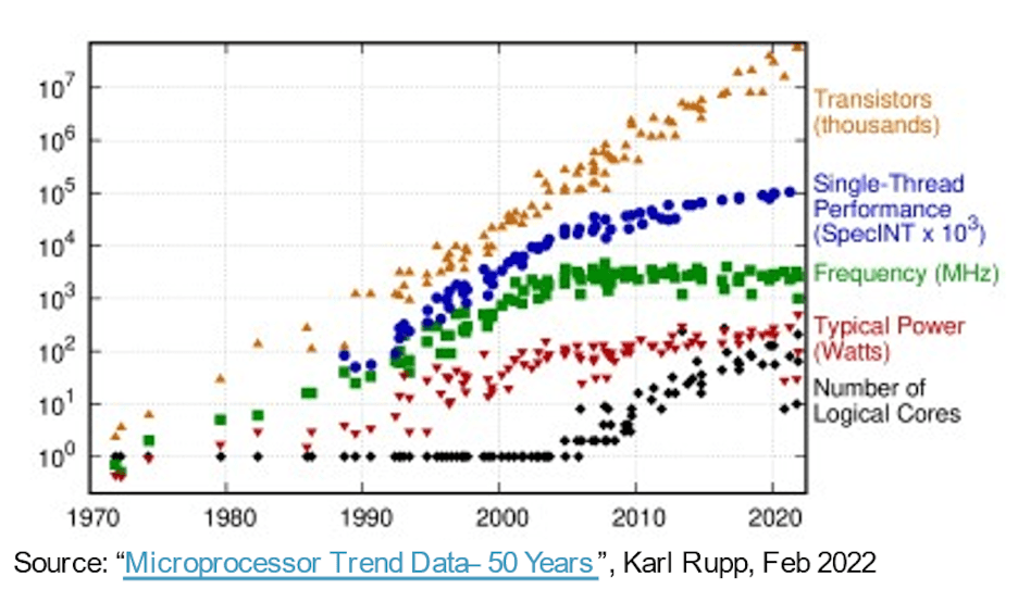
In the march to more capable, faster, smaller, and lower…
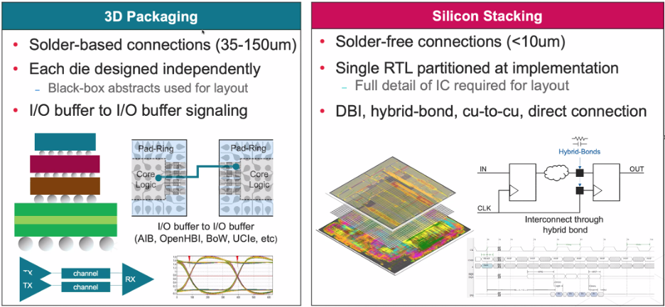
While terms often are used interchangeably, they are very different technologies with different challenges.
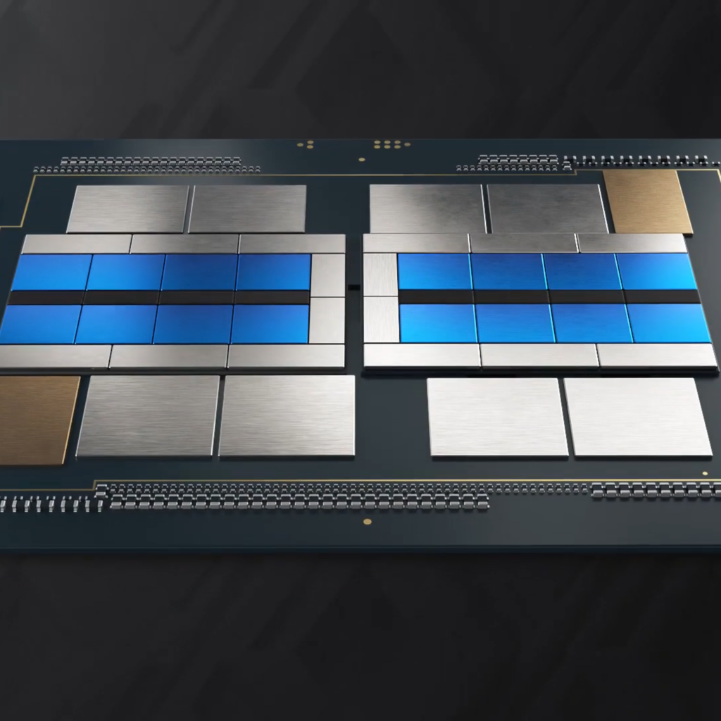
Historically Intel put all its cumulative chip knowledge to work advancing Moore's Law and applying those learnings to its future CPUs. Today, some of

Intel's multi-die interconnect bridge (EMIB) is an approach to in-package high-density interconnect of heterogeneous chips.

Powered by the promises of the CHIPS Act, Intel is investing more than $100 billion to increase domestic chip manufacturing capacity and capabilities.
If a few cores are good, then a lot of cores ought to be better. But when it comes to HPC this isn’t always the case, despite what the Top500 ranking –

Interconnects—those sometimes nanometers-wide metal wires that link transistors into circuits on an IC—are in need of a major overhaul. And as chip fabs march toward the outer reaches of Moore’s Law, interconnects are also becoming the industry’s choke point.
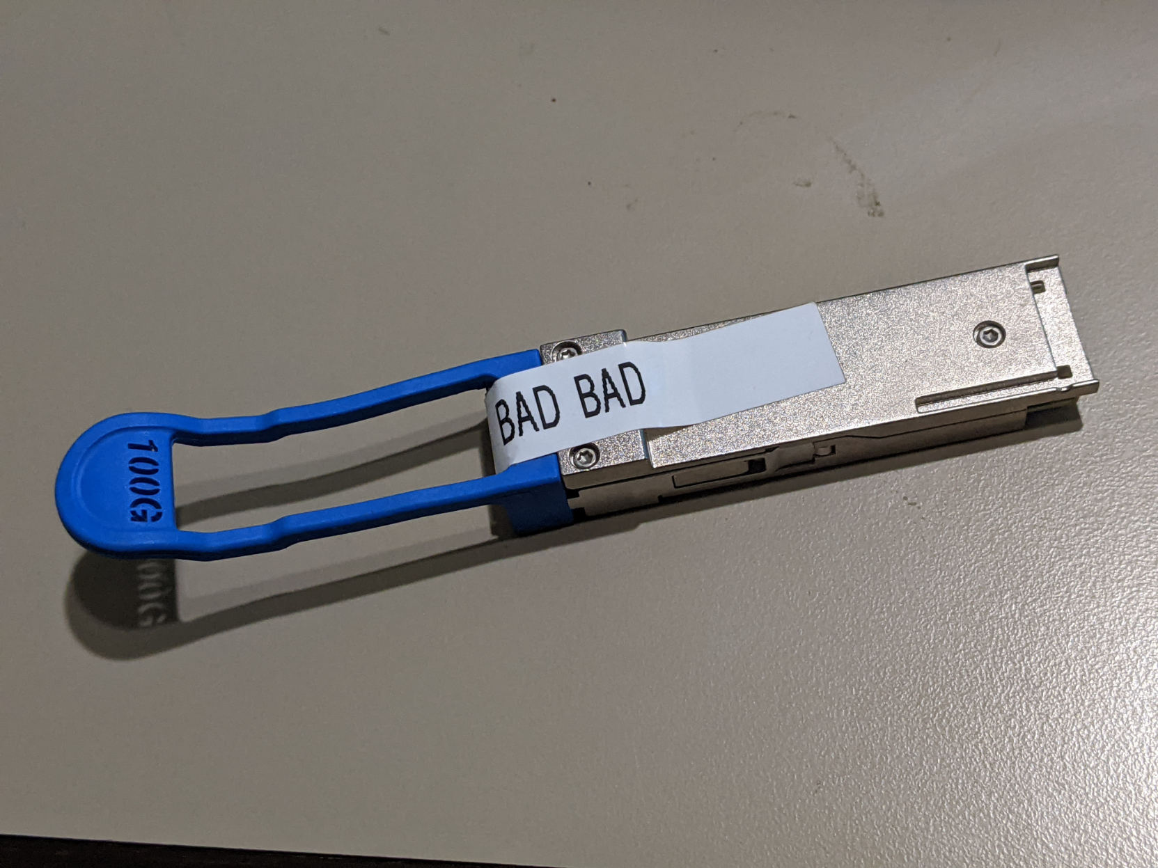
Attached: 2 images One of my nice friends at Hurricane Electric gave me a dead 100G-LR4 optic to tear apart for your entertainment, so for the sake of your entertainment, lets dig into it! 🧵
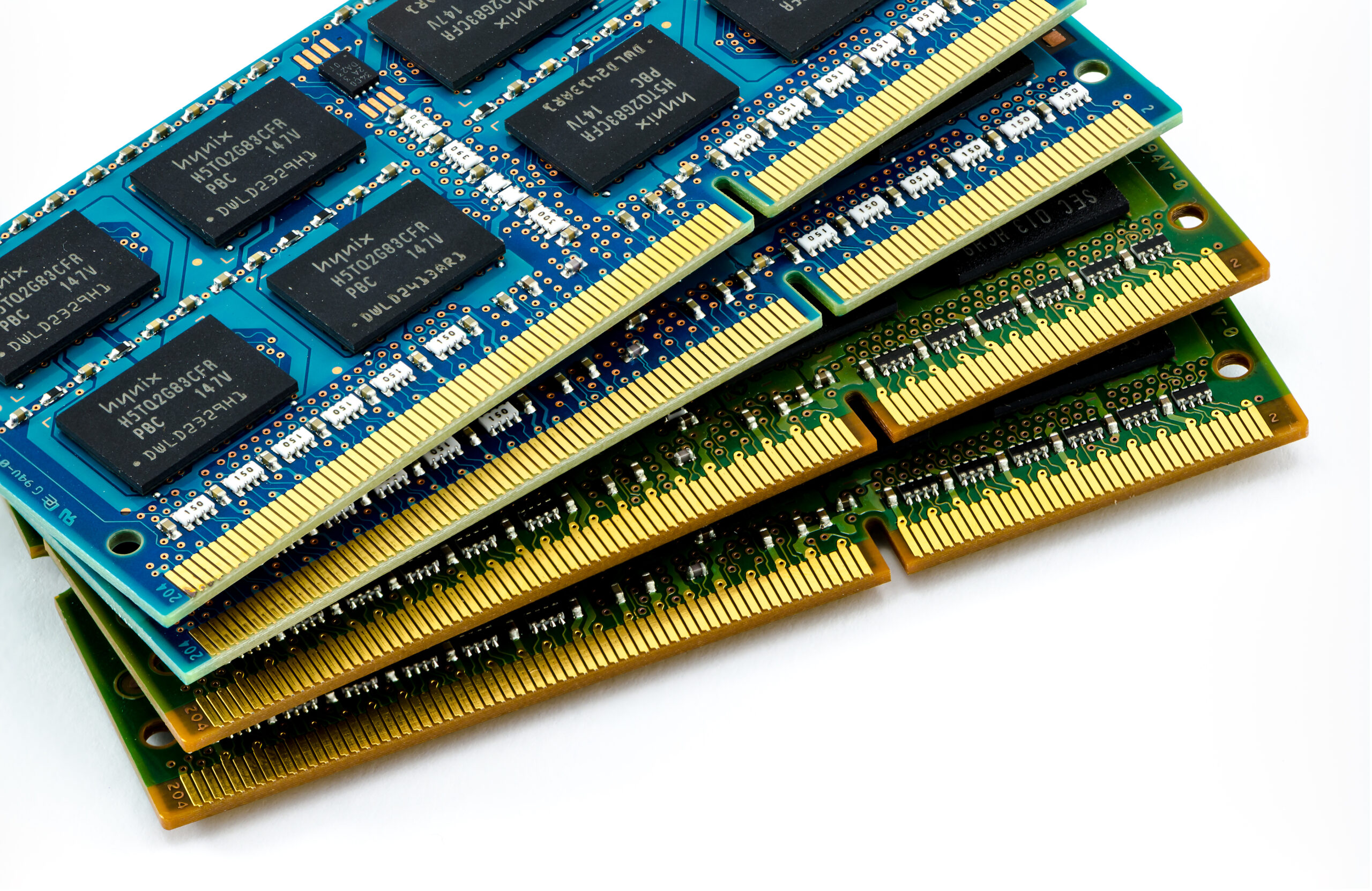
Conventional wisdom says that trying to attach system memory to the PCI-Express bus is a bad idea if you care at all about latency. The further the memory

The world's largest chip scales to new heights.
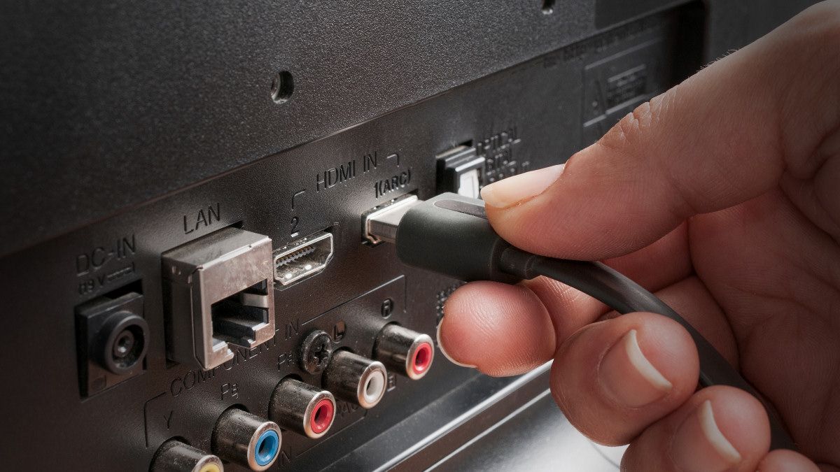
Get crystal-clear video and pristine audio with a single cable.

Let's learn more about the world's most important manufactured product. Meaningful insight, timely analysis, and an occasional investment idea.
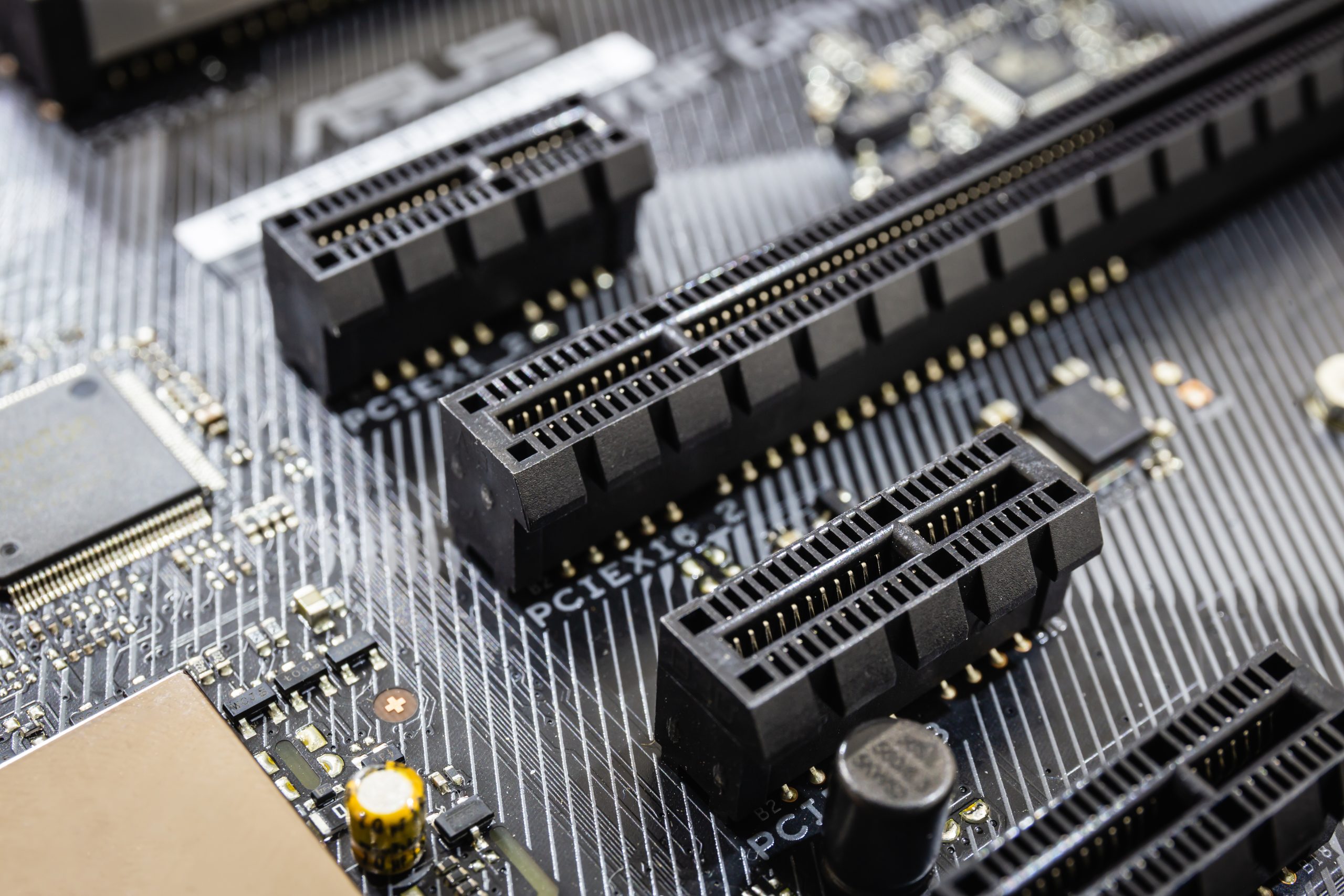
PCI-SIG has drafted the PCIe 7.0 spec and aims to finalize it in 2025.

Star Trek's glowing circuit boards may not be so crazy