The Tragedy of 3D XPoint (AKA Intel Optane AKA Micron QuantX)
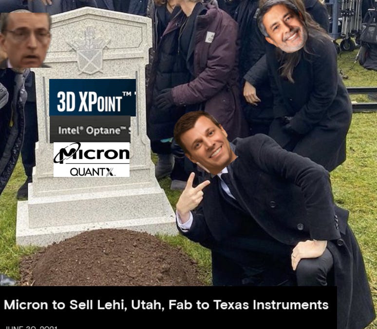
Too early and too late. Can it be resurrected from the dead?
Too early and too late. Can it be resurrected from the dead?

Kepler Computing claims a new approach to chip design—and a proprietary material—can help end the supply bottlenecks that have sent memory prices surging.

d-Matrix is tackling the 3D DRAM heat problem by stacking memory beneath the XPU, but atomic-level flatness remains a brutal barrier.
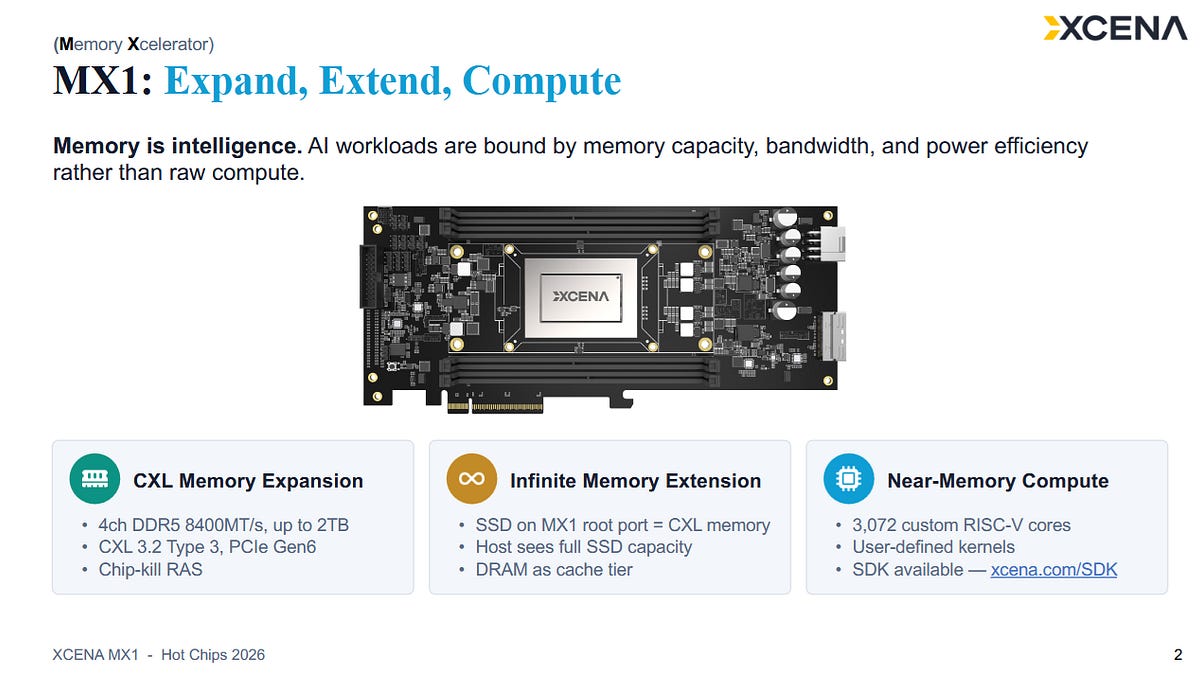
CXL memory expansion, with a side of compute
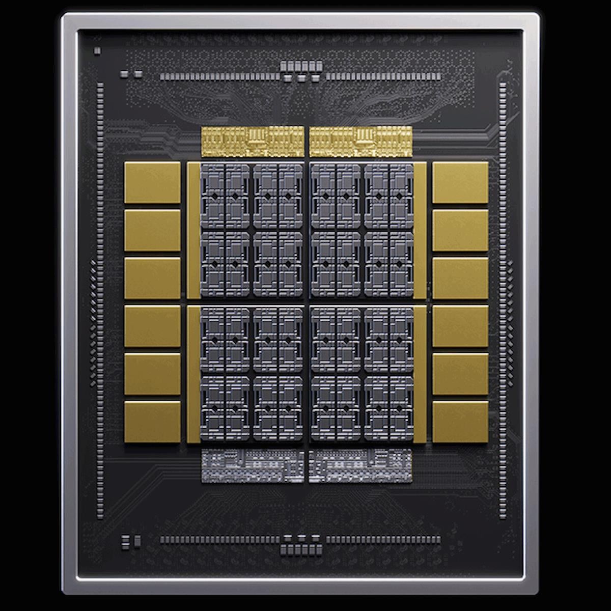
NVIDIA's NVHBM is a new memory technology that partners can license, offering improved efficiency and performance over standard HBM.
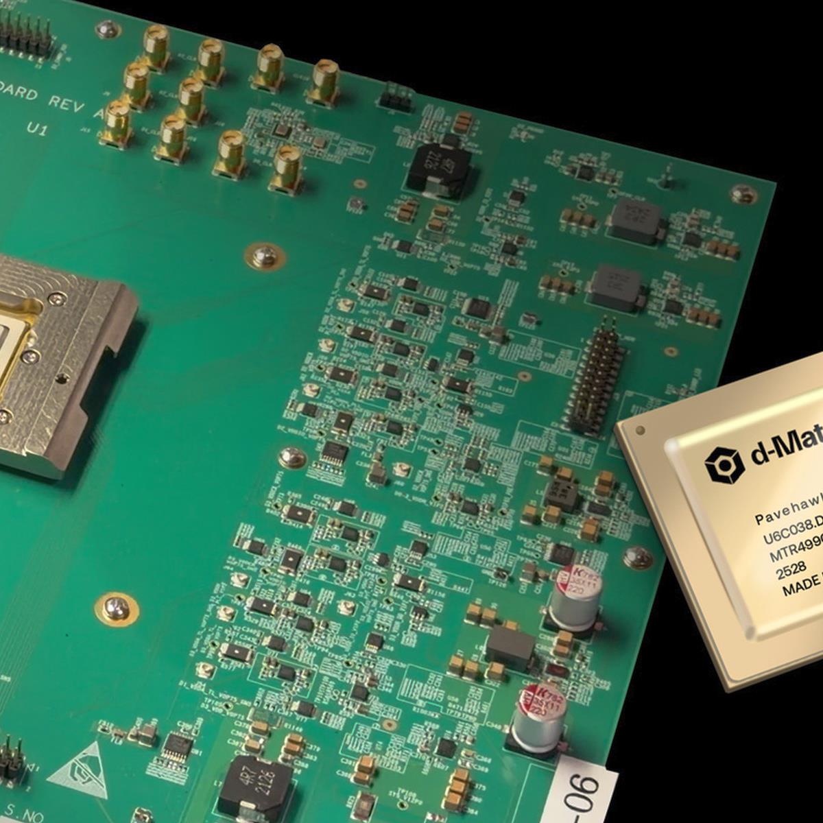
The company's ideas aren't novel, but it has solved long-standing challenges with 3D DRAM technology.

d-Matrix's Raptor 3D DRAM delivers 100 TB/s bandwidth at 0.37 pJ/bit, offering a high-efficiency alternative to SRAM and HBM for AI workloads
A look at AI Chip Architectures. NVIDIA, AMD, TPUs, Trainium, Groq, Cerebras.
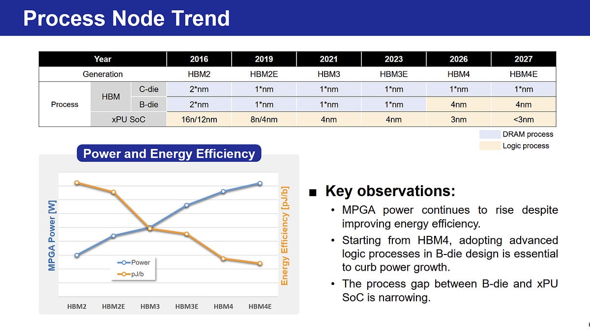
Machine learning applications demand ever more memory capacity and bandwidth. Samsung responded by fabricating their HBM base dies on a logic node, which opens up more opportunities
Wafer starts, die size, yield, HBM mix, node migration impacts, etc. Simple enough to follow, but detailed enough to learn from.
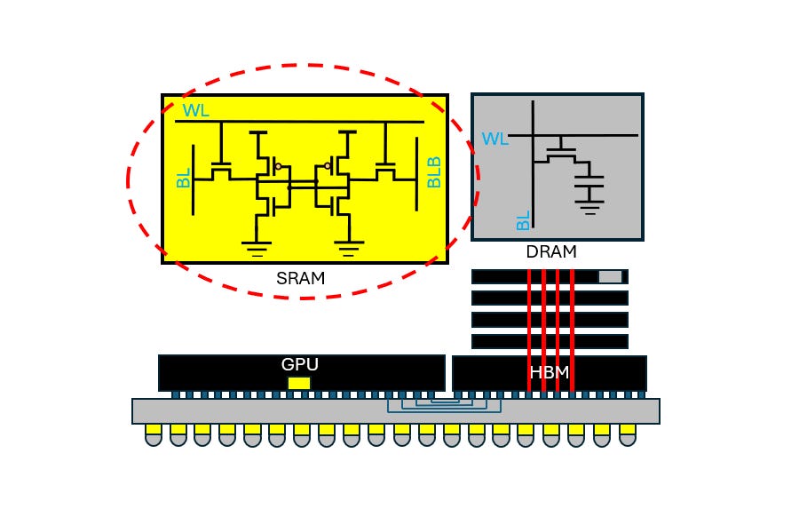
Fundamentals of SRAM and how SRAM constraints affect array size scaling and LLM inference performance

HBM manufacturing complexities are keeping general-purpose DRAM as Micron’s main cash cow, with DRAM gross margins projected to reach 95% by 2027

Why would a perfectly good plane suddenly go rogue? The answer was disturbing enough to ground 6,000 aircraft.

DRAM read disturbance, like RowHammer and RowPress, is a critical robustness issue where accessing DRAM can cause unintended bitflips in other unaccessed DRAM locations. DRAM read disturbance bitflips significantly impact the safe, secure, and reliable operation of DRAM-based…
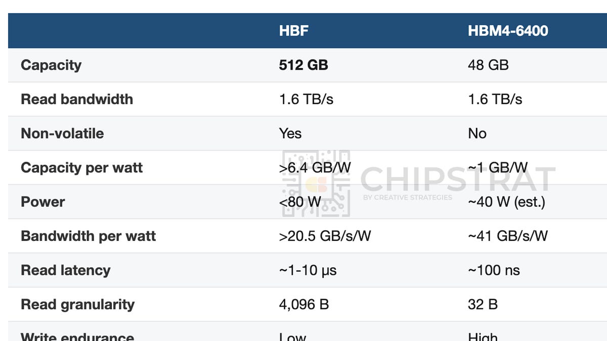
Why HBF for inference decode fits, what it does to the DRAM and NAND markets, a worked cost model, who moves first, and risks

High Bandwidth Flash offers efficient storage for model weights

CEA-Leti’s François Andrieu said it is pushing FeRAM because it could offer a useful combination of density, high endurance, and high speed.

Hamming Codes ECC RAM corrects errors that occur in memory before it gets to the CPU. The most common form of ECC is the Hamming Code [1] which when it has R redundant bits can correct single bit e…

What does a memory compiler actually do? From T-diagrams and 6T bitcells to GDS tiling, LVS, and the symmetry between memory compiler tiling and ML compiler tiling.
Kioxia and Sandisk haVE started delivering samples of its tenth generation 3D NAND BiCS chips w ...
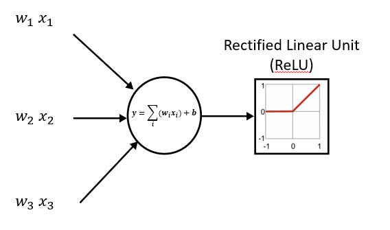
Learning from a classic AI accelerator - Eyeriss

Intel announced this week that it’s working with SoftBank subsidiary SAIMEMORY to commercialize Z-Angle Memory (ZAM), an advanced type of DRAM that stacks memory modules vertically. While ZAM chips aren’t expected to become available for at least three years, they could…
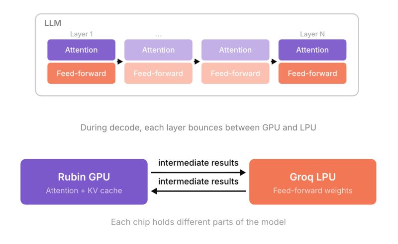
why did NVIDIA cancel the Rubin CPX and replace it with a Groq LPU? LLM inference has two phases. prefill processes the whole prompt at once and is compute-bound. decode generates one token at a time and is memory-bound, reading the full model weights and KV cache for every…

Disaggregated inference started as a software technique for splitting prefill and decode onto separate GPU pools. NVIDIA, Groq, Cerebras, and AWS are now taking it further with chips purpose-built for each phase.
prefill-decode disaggregation
production LLM serving

HBM, GDDR, and SRAM compared: how memory hierarchy, bandwidth, and capacity determine AI accelerator performance, cost, and which workloads each chip can serve.
prefill (processing the prompt), which is often compute-bound
decode (token-by-token generation), which is usually memory-bound

Samsung has reportedly produced the world's first standalone DRAM module that uses a process tech below 10nm.
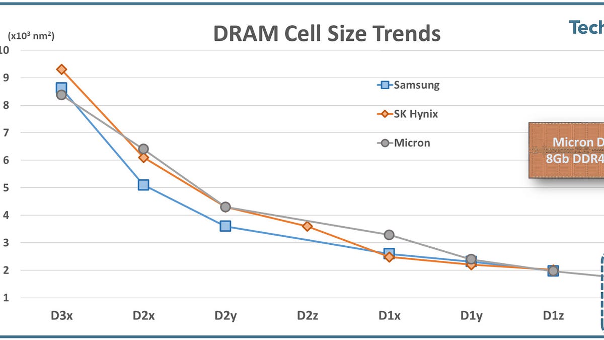
Note: The “1x, 1y, 1z, 1a…” naming is just the DRAM industry’s generational shorthand — each step is a shrink within the broad “10nm-class” umbrella, not a distinct architecture change. The progression: |Gen|Approx. node|Era | |---|------------|---------------------------| |1x |~18–19nm |~[2016–2017](tel:2016-2017)| |1y |~17nm |~2018 | |1z |~15–16nm |~[2019–2020](tel:2019-2020)| |1a |~14nm |~2021 | |1b…

DRAM Market Shift: From Mobile to Infrastructure (2023–2030) The latest DRAM demand outlook highlights a clear structural transition: memory demand is moving from mobile-driven to infrastructure-driven growth. 1. Infrastructure Becomes Dominant Servers & Workstations grow from…

🚨 DDR4 / LPDDR4: The Beginning of the End — or a Strategic Reset? The memory industry is approaching a pivotal inflection point—and the signals are becoming impossible to ignore. Recent developments from Samsung indicate that legacy nodes such as LPDDR4 (and increasingly DDR4)…

Rambus has announced its LPDDR5X SOCAMM2 memory chipset, a vital component to enable the next-gen compact memory for AI datacenters.

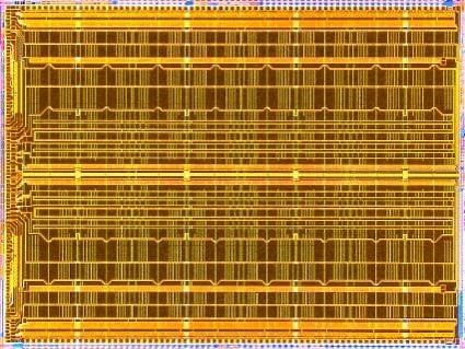
A new embedded memory architecture with a three-transistor cell.

Explore the four key modern memory types: ROM, DRAM, SRAM, and flash, their unique roles, and trade-offs in speed, cost, and storage.

A new technical paper titled “Functionally-Complete Boolean Logic in Real DRAM Chips: Experimental Characterization and Analysis” was published by researchers at ETH Zurich. Abstract: “Processing-using-DRAM (PuD) is an emerging paradigm that leverages the analog operational…
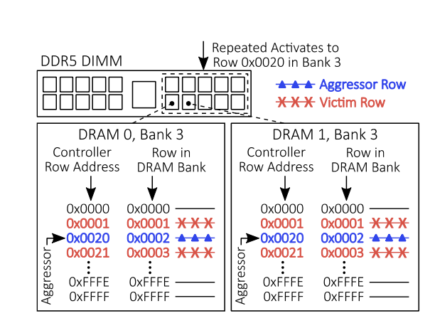
What it is, and why this has become such a significant security issue.
Need a New Year's resolution? How about stop paying for memory you don't need

Katherine Bourzac / IEEE Spectrum: The Northwest-AI-Hub, which is researching hybrid gain cell memory that combines DRAM's density with SRAM's speed, gets a $16.3M CHIPS Act grant via the US DOD