chip-design
174 bookmarks · page 1 of 4
2026-09-26 · arxiv.org

Complementary FETs (CFETs) extend nanosheet FET (NSFET) scaling by vertically stacking n- and p-type gate-all-around (GAA) devices, thereby shrinking standard-cell area. The performance gain, however, cannot be assessed from device metrics alone, as CFET layouts also introduce…
Note: Summary: This arXiv paper compares two next-generation chip technologies — A7 CFET and A10 NSFET — using a physics-based evaluation flow spanning from cell parasitics up to full-chip reliability. Approach: CFETs stack n- and p-type devices vertically to shrink cell area, but add extra cell-level resistance and capacitance. The authors built a flow linking calibrated device models, standard-cell…
2026-09-15 · spectrum.ieee.org

Today’s tidal wave of queries is forcing hardware makers to pivot
Note: ### The AI Inference Revolution Is Here [IEEE Spectrum article](#rid:1854764141) — a survey of how the shift from AI training to AI **inference** is reshaping chip and memory design. **The shift** Since 2020, the AI story was about training ever-bigger models. In 2026 the spotlight has moved to inference — putting trained models to work. People actually use LLMs now, reasoning models run…
2026-09-14 · spectrum.ieee.org

AI drastically shortened its design time; it will only get faster
2026-09-10 · semiengineering.com

How design-aware monitor analytics connects production measurements with device behavior and pre-silicon expectations.
2026-09-05 · yosyshq.readthedocs.io
2026-09-05 · pradyun.net
2026-09-04 · semiwiki.com
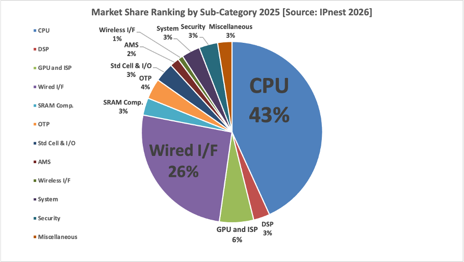
The $9.45 billion global design IP budget is distributed across 12 distinct sub-categories, heavily dominated by two primary pillars: CPU...
2026-09-02 · wccftech.com

A leaked Apple A20 Pro die shot reveals a record GPU core count for upgraded graphics, while new WMCM packaging unlocks a wider 96-bit memory bus width
2026-09-01 · wccftech.com

d-Matrix is tackling the 3D DRAM heat problem by stacking memory beneath the XPU, but atomic-level flatness remains a brutal barrier.
2026-08-30 · sciencedaily.com

Researchers have created a tiny chip that produces a stable “rainbow” of light capable of generating multiple high-frequency signals at once, potentially boosting the speed and capacity of future 6G networks. Its extreme precision could also make it valuable for quantum timing…
2026-08-30 · open.substack.com
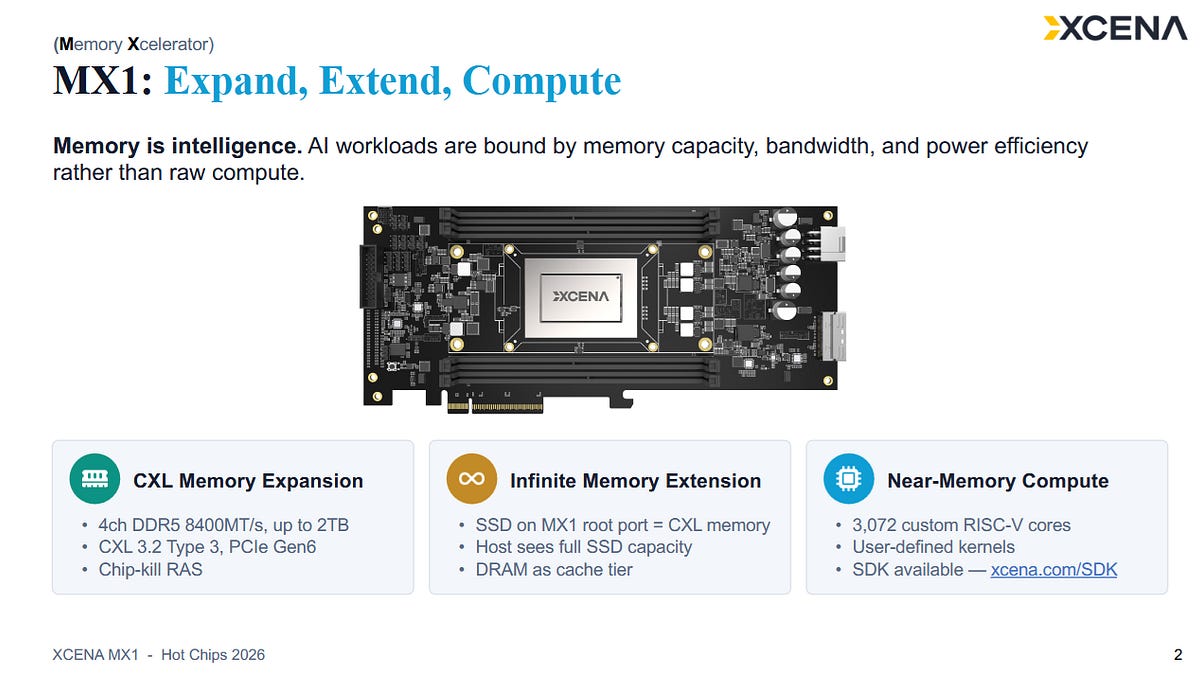
CXL memory expansion, with a side of compute
2026-08-24 · hothardware.com
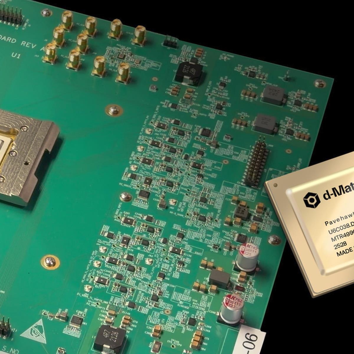
The company's ideas aren't novel, but it has solved long-standing challenges with 3D DRAM technology.
2026-08-24 · wccftech.com

d-Matrix's Raptor 3D DRAM delivers 100 TB/s bandwidth at 0.37 pJ/bit, offering a high-efficiency alternative to SRAM and HBM for AI workloads
★ 2026-08-24 · jepeake.com
A look at AI Chip Architectures. NVIDIA, AMD, TPUs, Trainium, Groq, Cerebras.
2026-08-19 · heyitshyam.substack.com
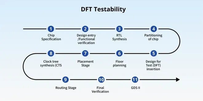
Designing a semiconductor chip is not only about making it perform its intended function.
2026-08-16 · linkedin.com
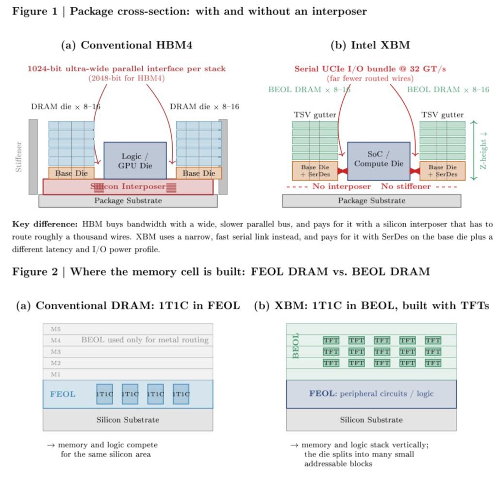
The most expensive part of HBM is not the DRAM. It is the piece of silicon underneath it. HBM moves data over a very wide parallel bus, roughly 1024 bits per stack. Every one of those wires has to be routed through a silicon interposer sitting between the memory and the compute…
2026-08-14 · open.substack.com
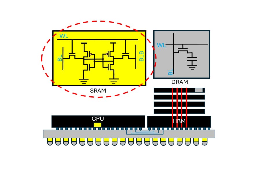
Fundamentals of SRAM and how SRAM constraints affect array size scaling and LLM inference performance
2026-08-09 · nextplatform.com
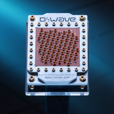
When D-Wave bought Quantum Circuits for $550 million in the early days of this year, it marked a sig ...
2026-08-06 · theregister.com

Early tech demos show model-specific integrated circuits churning out up to 17,000 tokens a second
2026-08-02 · chipsandcheese.com
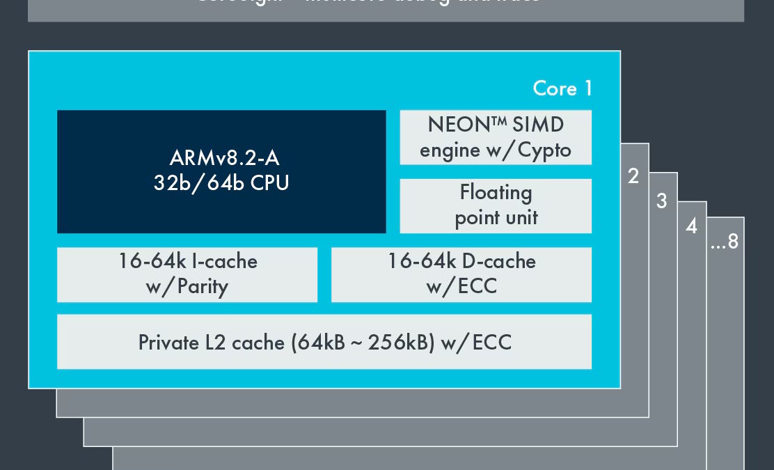
Arm’s 5-series cores are meant for tasks where performance barely matters, but power and area efficiency are top priorities.
2026-07-29 · risingedge.pro

Learn digital hardware design in the browser: write VHDL, Verilog and SystemVerilog, run real simulations, read waveforms, and see your RTL synthesized to a netlist. The skills behind FPGA and ASIC design, no installation required.
2026-07-27 · wccftech.com

Cadence has announced that its AI-driven digital and custom reference flows, tools, and solutions are now Intel 18A-P & 14A certified.
2026-07-26 · open.substack.com
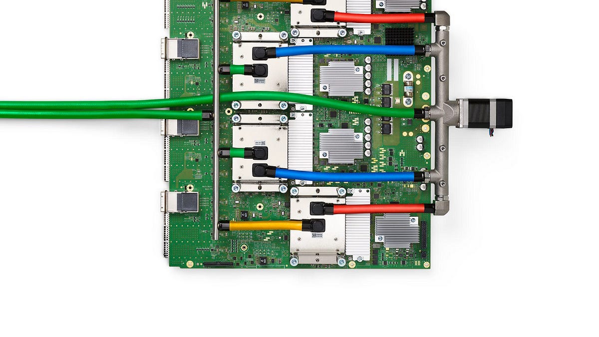
A sample of the designs that followed Google's first Tensor Processing Unit.
2026-07-15 · open.substack.com
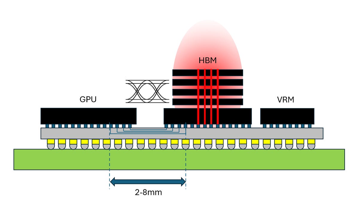
How transmission line effects and power-supply induced jitter make high-speed HBM interconnect scaling one of the most challenging co-design issues in AI racks
2026-07-12 · linkedin.com
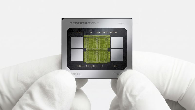
tensordyne just announced their chip specs. their trick is to turn every multiply into an add using logarithms, a trick from 1962 that everyone tried and gave up on. here's the breakdown: the idea is simple. log(a×b) = log(a) + log(b). store your numbers as logs and every…
2026-07-08 · rambus.com
Read this blog to learn what PCI Express is, how PCIe 7.0 improves bandwidth and efficiency, and how features like PAM4, FEC, FLIT mode and AXI support next-generation AI, cloud, HPC and edge systems.
2026-07-02 · chipify.io
Note: RF design?
2026-06-29 · cpushack.com
2026-06-27 · spectrum.ieee.org
Freed from intelligibility and aesthetics, AI designs faster
2026-06-26 · nextplatform.com
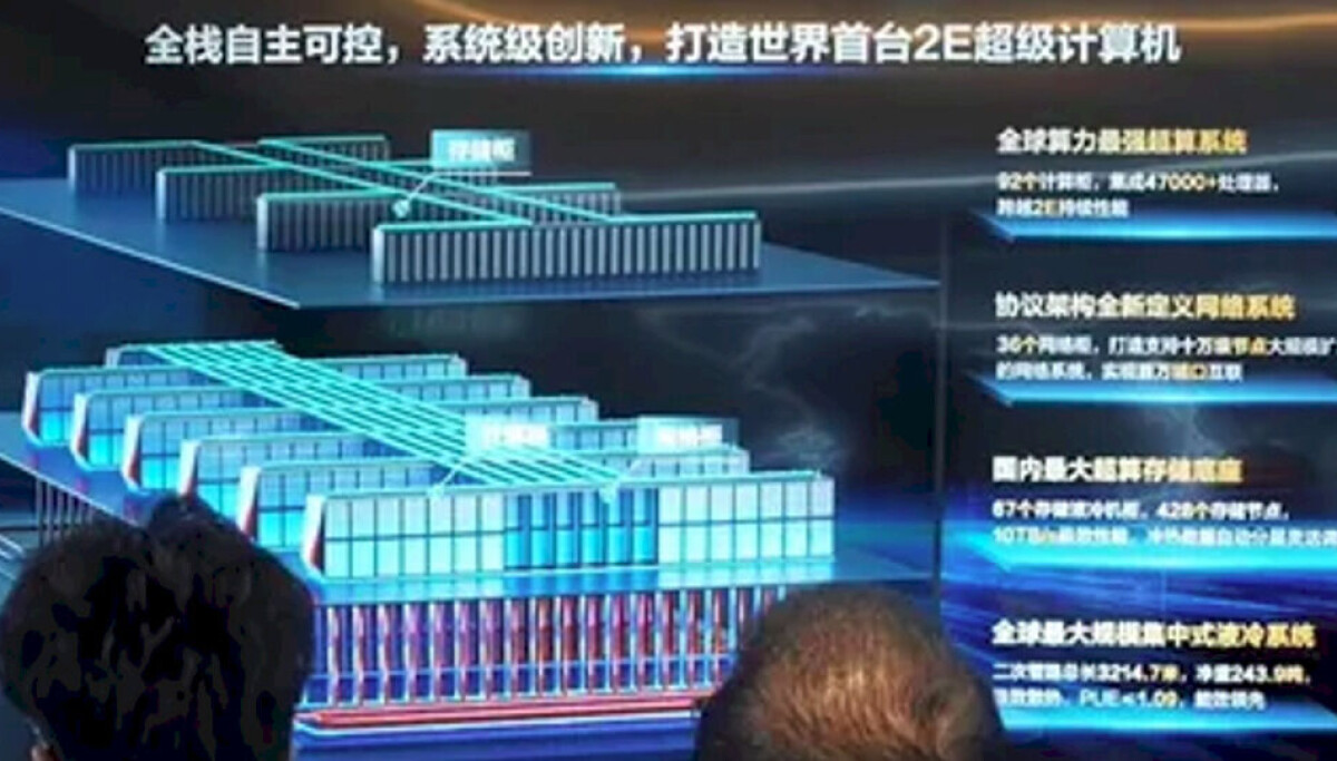
It has been nine years since a Chinese HPC supercomputer was at the top of the High Performance Linp ...
2026-06-25 · open.substack.com
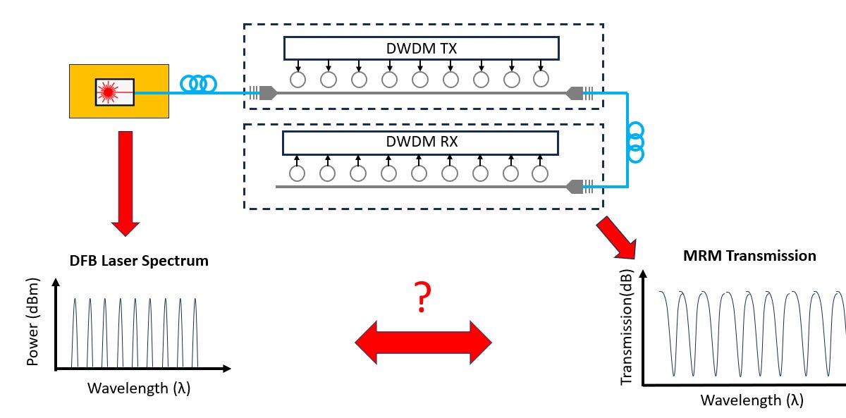
Key physics constraints and architecture challenges for scaling data rates in DWDM - ring modulator physics, clocking, CW-DFB Laser, and package integration
2026-06-15 · github.com
Library of open source PDKs
2026-05-29 · dataconomy.com

NASA's High Performance Spaceflight Computing project aims to significantly enhance the computational capabilities of spacecraft, enabling autonomous operations and faster
2026-05-24 · open.substack.com
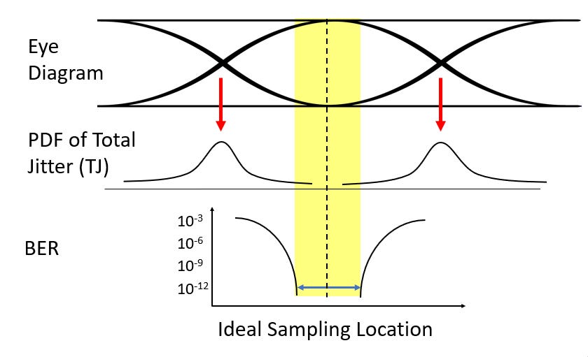
How signal integrity influences complexity of modern wireline transceiver architecture from first principles
2026-05-20 · open.substack.com
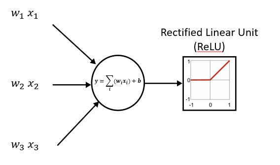
Learning from a classic AI accelerator - Eyeriss
2026-05-18 · open.substack.com
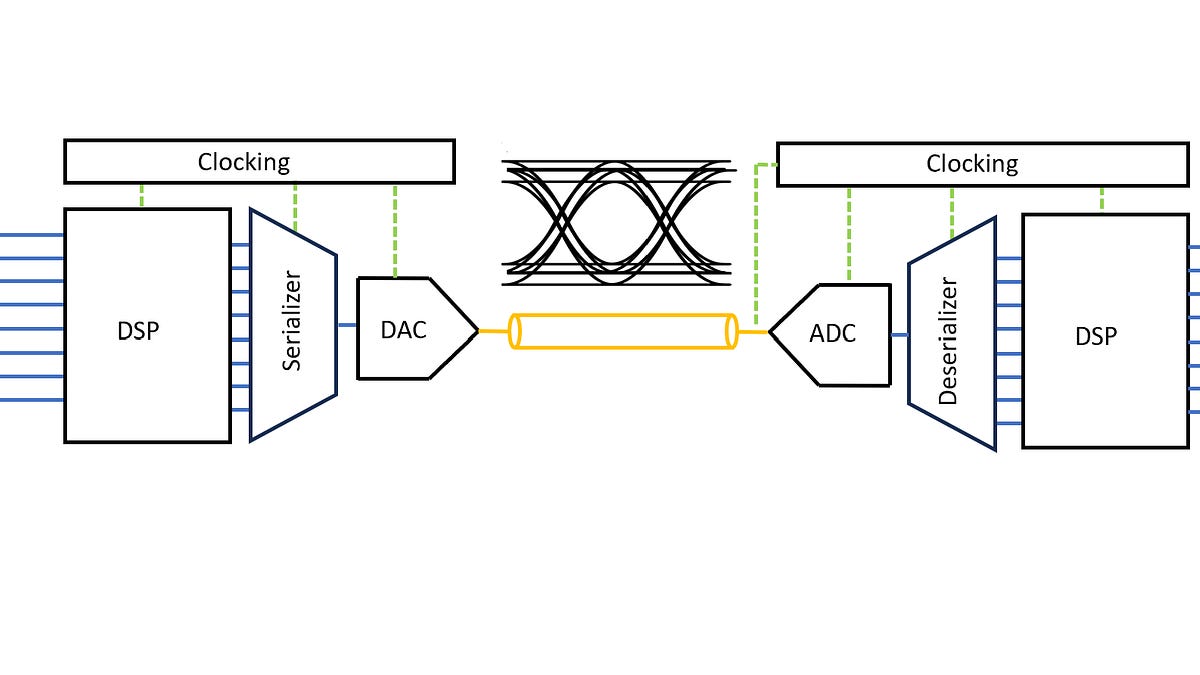
How high-speed data requirements influence chip architectural complexity
2026-05-12 · open.substack.com
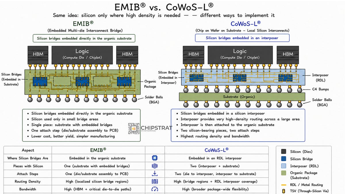
Is Intel's EMIB better than TSMC's CoWoS for AI accelerators? A primer on both, an honest look at the trade-offs, and where it goes from here.
★ 2026-05-12 · open.substack.com
Laying the Groundwork of the Current Chip Design Paradigm
2026-05-12 · en.wikipedia.org
file format used for specification of data structures for photomask production
2026-05-08 · open.substack.com

Q&A with SiTime CEO Rajesh Vashist
2026-05-04 · open.substack.com
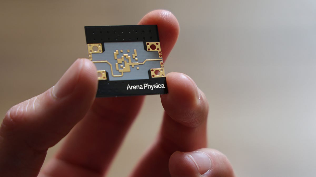
Tribal knowledge of RF design, EV range vs. temperature on the dyno, OpenAI's expanding robotic division, and more.
2026-04-29 · amcompute.com

Disaggregated inference started as a software technique for splitting prefill and decode onto separate GPU pools. NVIDIA, Groq, Cerebras, and AWS are now taking it further with chips purpose-built for each phase.
prefill-decode disaggregation
production LLM serving
★ 2026-04-29 · amcompute.com

HBM, GDDR, and SRAM compared: how memory hierarchy, bandwidth, and capacity determine AI accelerator performance, cost, and which workloads each chip can serve.
prefill (processing the prompt), which is often compute-bound
decode (token-by-token generation), which is usually memory-bound
2026-04-28 · spectrum.ieee.org
Sparse computing enables leaner, faster AI
2026-04-26 · wccftech.com

Samsung has reportedly produced the world's first standalone DRAM module that uses a process tech below 10nm.
Note: The “1x, 1y, 1z, 1a…” naming is just the DRAM industry’s generational shorthand — each step is a shrink within the broad “10nm-class” umbrella, not a distinct architecture change. The progression: |Gen|Approx. node|Era | |---|------------|---------------------------| |1x |~18–19nm |~[2016–2017](tel:2016-2017)| |1y |~17nm |~2018 | |1z |~15–16nm |~[2019–2020](tel:2019-2020)| |1a |~14nm |~2021 | |1b…
2026-04-25 · spectrum.ieee.org

Startup Verkor.io’s agentic AI orchestrated the entire design process from a 219-word prompt
2026-04-25 · semiwiki.com
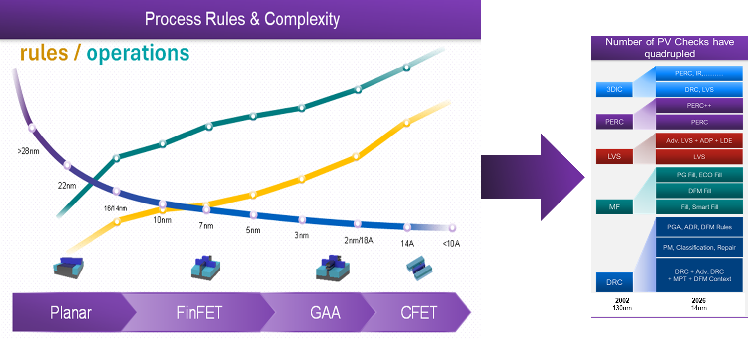
This blog looks at the details of how Synopsys IC Validator can overcome the advanced node physical verification bottleneck.
2026-04-20 · semiengineering.com
The cost case is strengthening, but glass, warpage, and bonding yield stand in the way.
2026-04-10 · marktechpost.com
2026-04-02 · semiengineering.com

A new embedded memory architecture with a three-transistor cell.